TSMC preps for ‘chiplet’ style manufacturing in 2021
CC Wei, CEO of TSMC, told analysts on a call to discuss first quarter financial results that: “We are also working with a few leading customers on SoIC, which is an industry-leading 3D-IC packaging solution. We target to start production in the 2021 time frame.”
Wei added that the packaging style was being well received in the mobile and high-performance computing sectors and that his company has an inquiry from an automotive chip company.
The SoIC manufacturing/packaging approach could be suitable for 5G, AI, IoT and automotive applications, according to EDA supplier Cadence Design Systems Inc.
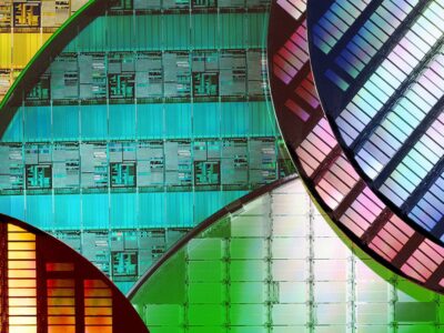
TSMC has offered a series of multi-die packaging options for several years including CoWoS [chip-on-wafer-on-substrate] and InFO [Integrated Fan-Out]. CoWoS made use of through silicon vias (TSVs) and was a high-performance option but its high expense meant it has received limited take up.
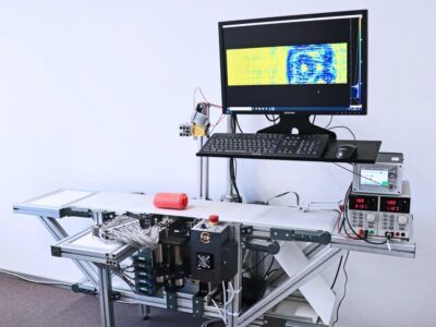
Meanwhile TSMC has been shrinking its manufacturing process technology. SoIC is a multi-chip stacking technology, which can be used with chips that are made using 10nm or finer manufacturing processes. It uses thermocompression bonding of copper-to-copper pads and supports both front and back bonding of die.
The absence of wire bonds means that smaller die can be sited close to each other on a larger die or on a silicon interposer. It also means that process technologies appropriate to different types of circuit; memory, logic, mixed-signal in a final packaged component that is about the same size as a monolithic die.
Previously the lower cost of minimal handling and higher reliability has always favoured monolithic integration. The absence of an EDA and packaging ecosystem to support it has also limited uptake, but several government and industry bodies are re-examining the chiplet approach chip manufacturing due to the extreme cost of leading-edge manufacturing.
Next: EDA support
The chiplet approach is likely to hinge on standardization of interfaces so that known-good-die (KGD) or chiplets can be placed in a library and then selected for assembly using die-to-die bonding. The result should make for quicker and lower cost design and assembly of complex chips.
Last month Cadence announced that TSMC had qualified its EDA tools as being suitable for the design SoICs . A full suite of Cadence digital and signoff, custom/analog, and IC package and PCB analysis tools have been optimized for TSMC’s SoIC chip stacking technology.
At the same time Ansys and Synopsys announced that their tools and design platform have been certified for SoIC chip-stacking technology.
Related links and articles:
News articles:
Broadcom preps for 7nm tape-outs in 2017
EDA tools support TSMC InFO 3D packaging
 If you enjoyed this article, you will like the following ones: don't miss them by subscribing to :