-600x400-c-default.jpg)
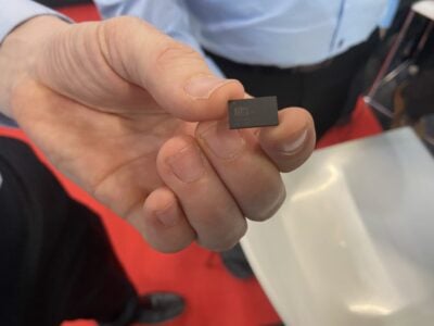
Infineon produce first silicon using 300-mm thin wafer technology for power semiconductors
The chips now produced on a 300-mm thin wafer exhibit the same behavior as the power semiconductors made on 200-mm wafers – as has been demonstrated by successful application tests using Metal Oxide Semiconductor Field-Effect Transistors (MOSFETs) for high voltage applications.
Infineon began setting up a power semiconductor pilot line for 300-mm wafer and thin wafer technology in Villach, Austria, in October 2010. The team today is composed of 50 engineers and physicists from the fields of research and development, manufacturing technology and marketing.
The first silicon on 300-mm is an achievement which, among other things, puts Infineon on track to continue its success story with power semiconductors used for energy efficiency applications.
As part of the investment plans, the company announced end of July 2011 to set up Dresden as the high volume production site for Power 300 technology. Infineon Technologies Dresden GmbH plans to invest around Euro 250 million for this purpose and will create 250 jobs in Dresden.
Infineon Technologies at www.infineon.com
 If you enjoyed this article, you will like the following ones: don't miss them by subscribing to :
eeNews on Google News


