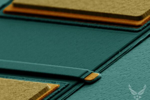
Developing FETs from gallium oxide
Gallium oxide (Ga2O3) has been around for many years as a conductive transparent film, but the wide bandgap of 4.5 to 4.9eV, compared to gallium nitride (GaN) at 3.3eV also means it can be used for high power switches. However, the material has been hard to work with.
“One of the largest shortcomings in the world of microelectronics is always good use of power: Designers are always looking to reduce excess power consumption and unnecessary heat generation,” said Gregg Jessen, principal electronics engineer at the Air Force Research Laboratory. “Usually, you would do this by scaling the devices. But the technologies in use today are already scaled close to their limits for the operating voltage desired in many applications. They are limited by their critical electric field strength.”
Jessen with fellow researcher Masataka Higashiwaki have been outlining a case for producing microelectronics using gallium oxide for field effect transistors (FETs) that could greatly benefit from gallium oxide’s large critical electric field strength. This would enable the design of FETs with smaller geometries and aggressive doping profiles that would destroy any other FET material says Jessen. Prototype diodes and RF and MODFETs have already been shown in the material.
“The next application for gallium oxide will be unipolar FETs for power supplies,” he said. “Critical field strength is the key metric here, and it results in superior energy density capabilities. The critical field strength of gallium oxide is more than 20 times that of silicon and more than twice that of silicon carbide and gallium nitride.”
Their research suggests that unipolar Ga2O3 devices such as the lateral FET shown above will dominate. “From a research perspective, gallium oxide is really exciting,” he said. “We are just beginning to understand the full potential of these devices for several applications, and it’s a great time to be involved in the field.”
The paper is plublished at AIP: https://doi.org/10.1063/1.5017845.
 If you enjoyed this article, you will like the following ones: don't miss them by subscribing to :
eeNews on Google News


