New class of layered materials drive PV innovations
According to the researchers, the approach is to design synergistic materials by combining two single-atom thick sheets, for example, acting as a photovoltaic cell as well as a light-emitting diode, converting energy between electricity and radiation. However, combining layers of atomically thin material is a thorny task that has flummoxed researchers for years.
The new material interlocks in a similar fashion to Lego bricks and the scientists’ findings are published by Nature Communications.
Hsin-Ying Chiu, assistant professor of physics and astronomy, and graduate student Matt Bellus fabricated the new material using ‘layer-by-layer assembly’ as a versatile bottom-up nanofabrication technique. Then, Jiaqi He, a visiting student from China, and Nardeep Kumar, a graduate student who now has moved to Intel Corp., investigated how electrons move between the two layers through ultrafast laser spectroscopy in the University of Kansas Ultrafast Laser Lab, supervised by Hui Zhao, associate professor of physics and astronomy.
“To build artificial materials with synergistic functionality has been a long journey of discovery,” Chiu said. “A new class of materials, made of the layered materials, has attracted extensive attention ever since the rapid development of graphene technology. One of the most promising aspects of this research is the potential to devise next-generation materials via atomic layer-level control over its electronic structure.”
“A big challenge of this approach is that, most materials don’t connect together because of their different atomic arrangements at the interface — the arrangement of the atoms cannot follow the two different sets of rules at the same time,” explained Chiu. “This is like playing with Legos of different sizes made by different manufacturers. As a consequence, new materials can only be made from materials with very similar atomic arrangements, which often have similar properties, too. Even then, arrangement of atoms at the interface is irregular, which often results in poor qualities.”
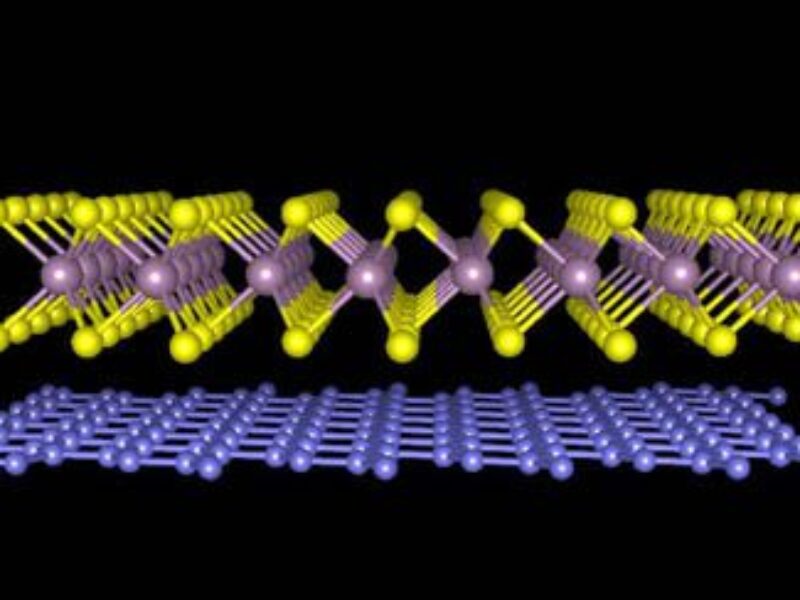
Layered materials such as those developed by the University of Kansas researchers provide a solution for this problem. Unlike conventional materials formed by atoms that are strongly bound in all directions, the new material features two layers where each atomic sheet is composed of atoms bound strongly with their neighbors — but the two atomic sheets are themselves only weakly linked to each other by the so-called van der Waals force, the same attractive phenomenon between molecules that allows geckos to stick to walls and ceilings.
“There exist about 100 different types of layered crystals — graphite is a well-known example,” Bellus said. “Because of the weak interlayer connection, one can choose any two types of atomic sheets and put one on top of the other without any problem. It’s like playing Legos with a flat bottom. There is no restriction. This approach can potentially product a large number of new materials with combined novel properties and transform the material science.”
Chiu and Bellus created the new carbon and tungsten disulfide material with the aim of developing novel materials for efficient solar cells. The single sheet of carbon atoms, known as graphene, excels at moving electrons around, while a single-layer of tungsten disulfide atoms is good at absorbing sunlight and converting it to electricity. By combining the two, this innovative material can potentially perform both tasks well.
The team used scotch tape to lift a single layer of tungsten disulfide atoms from a crystal and apply it to a silicon substrate. Next, they used the same procedure to remove a single layer of carbon atoms from a graphite crystal. With a microscope, they precisely laid the graphene on top of the tungsten disulfide layer. To remove any glue between the two atomic layers that are unintentionally introduced during the process, the material was heated at about 500 degrees Fahrenheit for a half-hour. This allowed the force between the two layers to squeeze out the glue, resulting in a sample of two atomically thin layers with a clean interface.
“We found that nearly 100 percent of the electrons that absorbed the energy from the laser pulse move from tungsten disulfide to graphene within one picosecond, or one-millionth of one-millionth second,” Zhao said. “This proves that the new material indeed combines the good properties of each component layer.”
The research groups led by Chiu and Zhao are trying to apply this Lego approach to other materials. For example, by combining two materials that absorb light of different colors, they can make materials that react to diverse parts of the solar spectrum.
Related articles and links:
News articles:
Can Fool’s gold reduce the cost of solar cells?
Graphene/nanotube cathode discovery enables cheaper dye-sensitized solar cells
Is graphene a real opportunity or just hype?
 If you enjoyed this article, you will like the following ones: don't miss them by subscribing to :