Integrated photonics advance promises next generation compute I/O
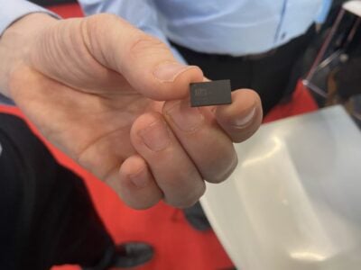
The latest research features industry-leading advancements in multiwavelength integrated optics, including the demonstration of an eight-wavelength distributed feedback (DFB) laser array that is fully integrated on a silicon wafer and delivers excellent output power uniformity of +/- 0.25 decibel (dB) and wavelength spacing uniformity of ±6.5% that exceed industry specifications.
“This new research demonstrates that it’s possible to achieve well-matched output power with uniform and densely spaced wavelengths,” says Haisheng Rong, senior principal engineer at Intel Labs. Most importantly, this can be done using existing manufacturing and process controls in Intel’s fabs, thereby ensuring a clear path to volume production of the next-generation co-packaged optics and optical compute interconnect at scale.”
This advancement, says the organization, will enable the production of the optical source with the required performance for future high-volume applications, such as co-packaged optics and optical compute interconnect for emerging network-intensive workloads including artificial intelligence (AI) and machine learning (ML). The laser array is built on Intel’s 300-millimeter silicon photonics manufacturing process to pave the way for high-volume manufacturing and broad deployment.
Silicon photonics is forecast to be be used in more than 20% of all high-bandwidth data center communications channels, up from less than 5% in 2020, which will represent a total available market of $2.6 billion. The growing demand for low power consumption, high bandwidth and faster data transfer is driving the need for silicon photonics to support data center applications and beyond.
With electrical interconnect performance limitations presenting an increasing challenge, integrating silicon circuitry and optics side by side on the same package holds the promise of a future input/output (I/O) interface with improved energy efficiency and longer reach. These photonic technologies were achieved in Intel’s fab using existing process technologies, which translates to favorable cost reductions of large-scale manufacturing.
Recent co-packaged optics solutions using dense wavelength division multiplexing (DWDM) technology have shown the promise of increasing bandwidth while significantly reducing the physical size of photonic chips. However, says the organization, it has been very difficult to produce DWDM light sources with uniform wavelength spacing and power until now.
This new advancement ensures consistent wavelength separation of light sources while maintaining uniform output power, resulting in meeting one of the requirements for optical compute interconnect and DWDM communication. The next generation of compute I/O using optical interconnect can be tailor-made for the extreme demands of tomorrow’s high-bandwidth AI and ML workloads.
The eight-wavelength DFB array was designed and fabricated using Intel’s commercial 300 mm hybrid silicon photonics platform, which is used to manufacture production optical transceivers in volume. This innovation, says the organization, marks a significant advancement in the capabilities of laser manufacturing in a high-volume complementary metal-oxide-semiconductor (CMOS) fab by utilizing the same lithography technology used to manufacture 300 mm silicon wafers with tight process control.
For this research, the company used advanced lithography to define the waveguide gratings in silicon prior to the III-V wafer bonding process. This technique resulted in better wavelength uniformity compared to conventional semiconductor lasers manufactured in 3-inch or 4-inch III-V wafer fabs. In addition, due to the tight integration of the lasers, the array also maintains its channel spacing when the ambient temperature is changed.
Looking forward, says the organization, core technology building blocks under development include light generation, amplification, detection, modulation, CMOS interface circuits and package integration technologies. In addition, many aspects of the eight-wavelength integrated laser array technology are being implemented by the company’s Silicon Photonics Products Division as part of a future optical compute interconnect chiplet product.
The forthcoming product will offer power-efficient, high-performance multi-terabits per second interconnect between compute resources including CPUs, GPUs and memory. The integrated laser array is a critical element to achieving a compact and cost-effective solution that supports high-volume manufacturing and deployment.
 If you enjoyed this article, you will like the following ones: don't miss them by subscribing to :
eeNews on Google News


