Understanding linear regulators and their key performance parameters
Low-dropout regulators, commonly known as LDOs, are used extensively in a wide variety of electronic applications across many different industries. An LDO is generally perceived as a simple and inexpensive way to regulate and control an output voltage that is delivered from a higher input voltage supply. However, cost and simplicity are not the only reason for their widespread use. In fact, today’s systems are getting more complex, noise sensitive and power hungry with every new design. The widespread use of
switching power supplies at all power levels means that designers must spend more time avoiding noise coupling and interference, while improving system efficiency, so cost and simplicity cannot be the only driver.
For most applications, a datasheet’s specifications of basic parameters are clear and easy to understand. Unfortunately, datasheets do not list the parameters for every possible circuit condition. Therefore, to make the best use of an LDO, it is necessary to understand the key performance parameters and their impact on given loads. Designers will need to determine whether the LDO is suitable for a specific load by closely
analyzing the surrounding circuit conditions.
This article examines the key performance parameters of LDOs and their impact on delivering clean output voltage to the various devices inside an electronic system.
We’ll also discuss the factors a designer must consider to optimize a system,
especially at higher current levels.
How LDOs are Used in Applications
In most applications, LDOs are primarily used to isolate a sensitive load from a noisy power source. Unlike switching regulators, linear regulators dissipate power in the pass transistor or the MOSFET that is used to regulate and maintain the output voltage to the required accuracy. As a result, an LDO’s power dissipation can be a significant disadvantage in terms of efficiency and can cause thermal issues. Therefore, it is important for designers to minimize LDO power dissipation to boost system efficiency
and avoid any thermal complications.
LDOs are one of the oldest and most commonly used devices for voltage regulation; however, many of their key performance parameters are not so well understood or at least not utilized to their full potential. While cost is a very important factor, the use of LDOs is primarily driven by the system’s power requirement and acceptable noise level of the load being powered. LDOs are also used for noise reduction, and to fix problems caused by electromagnetic interference (EMI) and PCB routing.
For very low current loads, an LDO’s power dissipation is very minuscule, so they become an obvious choice for their simplicity, cost and ease of use. However, for high current loads greater than 500mA, other factors become more important and sometimes even critical. In these types of applications, it is important for system designers to look at performance parameters that grow in importance at higher current levels, such as the dropout voltage, load regulation and transient performance.
Since LDOs are a type of linear regulator, they are often compared with traditional linear regulators, especially in terms of cost. It is important to understand that the pass element is the core of an LDO, and this core and its surrounding circuits dictate the LDO’s performance.
Inside the LDO
An LDO comprises three basic functional elements: a reference voltage, a pass element and an error amplifier, as shown in Figure 1. During normal operation, the pass element behaves as a voltage controller current source. The pass element is driven by a compensated control signal from the error amplifier, which senses the output voltage and compares it with the reference voltage. All of these function blocks affect the LDO’s performance. LDO manufacturers’ datasheets always include specifications that indicate the performance of these functional elements.

Figure 1: Block diagram of the LDO
As you can see in Figure 2, four different kinds of pass elements are typically found in LDO regulator designs: NPN transistor-based regulators, PNP transistor-based regulators, N-channel MOSFET-based regulators and P-channel MOSFET-based regulators.

(A) NPN transistor-based regulator (B) PNP transistor-based regulator

(C) N-Channel MOSFET-based regulator (D) P-Channel MOSFET-based regulator
Figure 2: Four different types of transistors used in LDO regulators
In general, transistor-based regulators have higher dropout voltage compared to MOSFET-based regulators. Additionally, a transistor-based regulator’s base driving current of the transistor pass element is proportional to the output current. This directly impacts the transistor-based regulator’s quiescent current. By comparison, the MOSFET pass element uses voltage driven on the isolated gate to make its quiescent current significantly lower than the transistor-based regulator.
Key LDO Performance Parameters
1) Dropout Voltage
Dropout voltage is defined as the difference between the input and output voltages at the point when a further decrease in input voltage causes output voltage regulation to fail. In the dropout condition, the pass element operates in the linear region and behaves like a resistor. For the modern LDO, the pass element is typically implemented with PMOS or NMOS FETs, which can achieve a dropout voltage as low as 30mV to 500mV.
Figure 3 shows the dropout voltage of the ISL80510 LDO, which uses a PMOS FET as the pass element.

Figure 3: ISL80510 dropout voltage
2) Load Regulation
Load regulation is defined as the output voltage change for a given load change. This is typically from no load to full load, given by Equation 1:
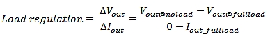
Load regulation indicates the performance of the pass element and the closed-loop DC gain of the regulator. The higher the closed-loop DC gain, the better the load regulation.
3) Line Regulation
Line regulation is the output voltage change for a given input voltage change, as defined in Equation 2:

Since line regulation is also dependent on the performance of the pass element and closed-loop DC gain, dropout operation is often not included when considering line regulation. Hence, the minimum input voltage for line regulation must be higher than the dropout voltage.
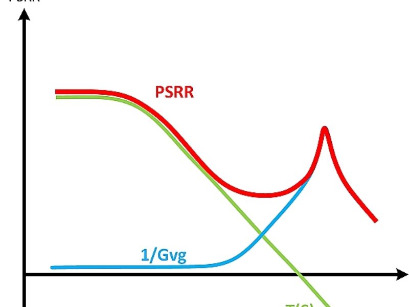
4) Power Supply Rejection Ratio (PSRR)
PSRR is an indication of the LDO’s ability to attenuate fluctuations in the output voltage caused by the input voltage, as expressed in Equation 3. While line regulation is only considered at DC, PSRR must be considered over a wide frequency range. Equation 3:

Considered a conventional closed-loop system, the small-signal output voltage, Ṽout , can be expressed as shown in Equation 4:

Where Ṽin is the small signal input voltage, Gvg is the open-loop transfer function from input to output voltage, kv is the output voltage sensing gain, Gc is the compensator’s transfer function, Goc is the open-loop transfer function from the control signal to the output voltage, and
kv x Gc x Goc is the closed-loop transfer function, T(s).
As we can see in Equations 3 and 4, it is clear that the PSRR consists of the closed-loop gain, T(s) , and the inverse of the open-loop transfer function from input to output voltage, 1/Gvg, as shown in Figure 4. While the closed-loop transfer function dominates at lower frequencies, the open-loop transfer function from input to output voltage dominates at higher frequencies.

Figure 4: PSRR vs. Frequency
5) Noise
This parameter normally refers to the noise on the output voltage generated by the LDO itself, which is an inherent characteristic of the bandgap voltage reference. Equation 4 shows the relation of the reference voltage to the output voltage. Unfortunately, the closed-loop transfer function is not effective at rejecting the noise from the reference voltage to the output voltage. Hence, most low-noise LDOs need an additional filter to prevent noise from entering the closed-loop.
6) Transient Response
LDOs are commonly used in applications where point-of-load regulation is important, such as powering digital ICs, DSPs, FPGAs and low-power CPUs. The load in such applications has multiple modes of operation, which require different supply currents. As a result, the LDO has to respond quickly to keep the supply voltage within the required limits. This makes the transient behavior of an LDO one of the critical performance parameters.
As in all closed-loop systems, the transient response mainly depends on the bandwidth of the closed-loop transfer function. To achieve the best transient response, the closed-loop bandwidth has to be as high as possible while ensuring sufficient phase margin to maintain stability.

Figure 5: ISL80510 transient response (2.2Vin, 1.8Vout)
7) Quiescent Current
The quiescent current (or ground current) of an LDO is the combination of the bias current and drive current of the pass element, and is normally kept as low as possible.
Additionally, when PMOS or NMOS FETs are used as the pass element, the quiescent current is relatively unaffected by the load current. Since the quiescent current doesn’t pass through to the output, it influences the LDO’s efficiency, which can be calculated as follows in Equation 5:
The power dissipation inside the LDO is defined by: Vin x (Iq + Iout) – Vout x Iout .
To optimize the LDO’s efficiency, both quiescent current and the difference between the input and output voltages must be minimized. The difference between the input and output voltages have a direct impact on efficiency and power dissipation, so the lowest dropout voltage is generally preferred.
Even though an LDO cannot deliver high efficiency conversion compared to a switching-mode power supply (SMPS), it is still a necessary voltage regulator for many modern applications. In noise sensitive applications, it is very challenging for an SMPS to achieve the necessary output ripple to meet a tight noise specification. Consequently, it is not uncommon for an LDO to be added as an active filter to the output of an SMPS. This LDO must have high PSRR at the SMPS switching frequency.
LDOs are particularly suited to applications that require an output voltage regulated to slightly below the input voltage. While buck and boost converters have limitations on the maximum/minimum duty cycle, their output voltage will lose regulation with an input voltage that is close to the output voltage.
Conclusion
Though simple in concept and implementation, widely used LDOs perform a vital function in system power design. There are many factors that need to be considered to optimize a design, particularly at higher current levels. For mid- to high‑current applications,
Intersil’s ISL80510/05 provides balanced performance across all key LDO performance parameters: low dropout, transient performance, voltage accuracy and a near flat PSRR response across a wide range of frequencies.
References
Learn more about the ISL85010/05.
Get the ISL85010 datasheet.
Watch a video overview of the ISL85010/05.
 If you enjoyed this article, you will like the following ones: don't miss them by subscribing to :