Triac triggering compliance: The basics of positive and negative supplies
Positive and negative power supplies
Non-insulated power supplies are often required when a power semiconductor, which has to be controlled using this supply, has its drive reference connected to the mains (line or neutral terminal).
This is the case, for example, for triggering an AC switch such as a Triac, ACST, ACS or SCR (Silicon Controlled Rectifier).These devices are all controlled by a gate current. This gate current has to be applied on the gate pin and circulates between the gate and the AC switch reference terminal, which is the Cathode (K) for SCR, A1 for Triac, or COM for ACST and ACS.
As the AC switch control circuit, and so its power supply, has to be referenced to the device reference terminal (connected back to the line voltage), a non-insulated power supply is required.
There are two ways to connect this drive reference to the non-insulated power supply:
- Solution 1: connect the control circuit ground (VSS) to drive reference.
- Solution 2: connect the control circuit voltage supply (VDD) to drive reference.

Figure 1: Supply polarity definition
Solution 1, shown in Figure 1a, is the most common solution, as the switch drive reference is also the zero voltage point (VSS). Such a topology is called a positive power supply as the voltage supply (VDD) is indeed above the mains terminal potential (line or neutral), which is connected to the drive reference (VSS).. If the supply is a 5 V power supply, then VDD is 5 V above the mains reference (neutral terminal in Figure 1a example).
This topology can be used directly only with standard Triacs and SCR, not with non-standard Triacs, ACS and ACST, as explained below. But some simple modifications can be implemented to control all these devices from a positive supply as explained at the end of this article.
Solution 2, shown in Figure 1b, is called a negative power supply. The voltage supply reference (VSS) is indeed below A1 or COM, which is connected to the mains reference. If the supply is a 5 V power supply, then VSS is 5 V below the line reference, or at – 5V compared to the line.
This topology can be used with all Triacs, ACS and ACST, but not with SCR, as explained below.
Compliance of supply output polarity with AC switch technology
To switch on an AC switch, like any bipolar device, a gate current must be applied between its gate pin (G) and its drive reference terminal (refer also to STMicroelectronics’ AN3168 application note).
Then several cases occur.
- For a SCR, this gate current has to be positive (circulating from G to K).
- For a Triac and an ACST, the gate current could be positive or negative (depending on the voltage applied to the device).
- For an ACS, the gate current has to be negative (circulating from COM to G).
An SCR can so be easily driven from a positive supply. If its Cathode is connected to VSS as it is on Figure 1a, a current will be sourced to the SCR gate when the Control Circuit (usually a microcontroller) output pin will be put at high level.
On the other hand, an ACS needs a negative supply to be directly driven as shown in Figure 1b. A current will thus be sunk from the SCR gate when the Control Circuit output pin will be put at low level.
For Triac, ACS and ACST, four triggering quadrants can be defined according to the polarity of the gate current and the polarity of the voltage applied across the device before turn-on. The gate current is counted as positive when it is sourced to the gate. The voltage is counted positive when referred to its drive reference. The different quadrants are
- Quadrant 1: positive gate current and positive voltage.
- Quadrant 2: negative gate current and positive voltage.
- Quadrant 3: negative gate current and negative voltage.
- Quadrant 4: positive gate current and negative voltage.
Triac, ACS and ACST devices can be triggered in each or only some of these quadrants according to their technology.
For an SCR, as only a positive gate current can switch-on the device and as it can only turn on when a positive voltage is applied across its Anode and Cathode terminals, the triggering quadrants are usually not considered for these devices.
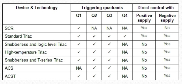
The following table shows the different quadrants for the different devices’ technologies and lists the power supply polarity compliance to allow a direct driving circuit as shown in Figure 1. As can be seen, a negative supply is compatible with all the AC switches’ technologies except SCR. A negative output is then preferred as it will allow a part number to be changed by any other technology.
Table 1: Devices’ triggering quadrants and compliance with direct control from positive or negative supply
Supply topology impact on output polarity
The problem occurs if one wants to trigger a 3-quadrant Triac, an ACST or an ACS, with a microcontroller unit (MCU) supplied with a positive voltage. Indeed, as shown in Table 1, a direct control cannot be implemented in this case.
Moreover, Switched Mode Power supplies (SMPS) are frequently being used to fit within the different directives or standards on stand-by power consumption. The choice of an SMPS with a positive output is often done mainly because it relies on the choice of a buck converter as it is the most common topology for low output current off-line converters
But there are many applications where only AC switches have to be controlled, and so a negative supply could be implemented. A buck-boost converter allows a negative output. Such a topology is as easy as a buck converter to implement. Furthermore, for a buck-boost converter, there is no need for an added output load resistance or output Zener as it is required for a buck topology. Indeed, for a buck the output capacitor is charged during each MOSFET on time, resulting in a too high output in case of no-load or very light load.
For a buck-boost converter, the efficiency (as well as the maximum output current) should be lower and the output capacitor bigger than for a buck converter. Indeed, the whole inductor current is used to charge the output capacitor for the buck converter, whereas for the buck-boost, the inductor current will charge the output capacitor only during the freewheeling times. But for a 230 V AC / 12 V DC converter, the duty cycle is very low, and there is no great difference between buck and buck-boost performances. Similar efficiency is reached for both topologies with the same reactive components.
But even if an SMPS with negative outputs is available, a positive output could be preferred. A positive output allows for lower power consumption in stand-by mode. Indeed, positive linear voltage regulators can be found with internal consumption in the range of 50 µA, while the typical consumption of a negative voltage regulator is around 2 mA. This quiescent current significantly affects the standby consumption of the SMPS.
Another reason to implement a positive output is that 3.3 V MCUs are promoted widely, and it is very difficult to find accurate 3.3 V negative voltage regulators with low consumption.
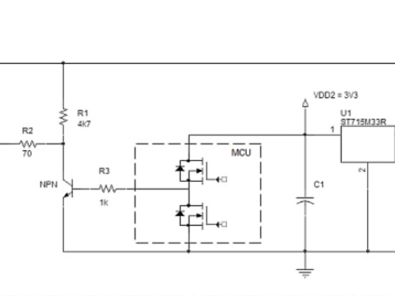
For these reasons, the Figure 2 schematic could be implemented to combine both the advantages of a negative power supply and the advantages of a positive voltage regulator. In this schematic, a ST715M33R positive regulator, which presents a 5.5 µA maximum quiescent current, is used to show the implementation of a 3.3V supply from a “negative” 15 V output, which could come from a buck-boost or a flyback converter implemented with a VIPer06 circuit (refer to STMicroelectronics AN4564 application note for further information). The MCU is then able to sink the current from the T1635T-8 Triac, a T-series 3-quadrant device.

Figure 2: Positive regulator used for negative supply of Triac control circuit
Adapt the gate circuit to drive a 3-quadrant Triac from a positive supply
There are other reasons, apart from the choice of power supply topology, which could lead to the need for a positive power supply.
It could be the case, for example, of applications where a sensor is referenced to the mains. This is done to monitor certain electrical parameters. For example, for universal motor controls, a shunt resistor is often added in series with the AC switch to sense the load current to implement a speed or torque closed-loop control. In power metering applications, the mains voltage must be measured in order to calculate the energy sunk from the grid.
Circuits are then traditionally implemented with a positive supply as it seems more logical to sense a voltage that increases when the shunt current or the line voltage also increases.
Such schematics can also be adapted to a negative supply. The MCU firmware logic has then to be adapted to take into account this reversed measurement (refer to AN4564).
In case a positive supply is definitely selected, there is still a solution to drive a 3-quadrant Triac, an ACS or an ACST. One solution is to simply add a capacitor (C1) in series with the gate resistor (R1), as shown on Figure 3a, to allow the current to be sunk from the Triac gate.
The principle of operation of this schematic is the following:
- when the MCU I/O pin is put to high level (VDD), capacitor C1 is charged through R1 and the Triac gate. As a 3-quadrant Triac could not be triggered in quadrant Q4, the Triac will not turn on if the voltage across terminals A2 and A1 is negative (but could turn on if this voltage is positive, in Q1 quadrant).
- when C1 capacitor is fully charged (to the MCU supply, which is 5 V here) the gate current disappears.
- when the MCU I/O pin is put to low level (VSS), C1 is discharged through R1 providing a negative current to the Triac gate. The Triac is then triggering in quadrants Q2 or Q3, respectively, if the voltage across its terminals is positive or negative. The negative current flows until the capacitor C1 is discharged.
Figure 3b gives a variant of Figure 3a schematic for the specific case of controlling an ACS device (like an ACS108 in this example). As such devices present a single P-N junction between their COM and G terminals that prevent any current flow sourced from G to COM, the D1 diode is added to allow the charge of the C1 capacitor when the MCU I/O pin is put at high level.

Figure 3: 3-quadrant Triac or ACS driving circuit with a positive supply
For both schematics, an alternative gate current is applied as long as the MCU I/O pin applies a burst voltage pulse. The advantage of such a control method is that the capacitor blocks the DC current that can appear in case of MCU disoperation due to reset or latch-up and increases the safety level of the application.
Conclusion
To fit with the different standards on stand-by power consumption, an SMPS is frequently being used. Power supplies with positive output are commonly implemented whereas a negative voltage could be preferred as the negative voltage will allow compliance with a wide range of AC switches.
Positive output could be preferred as voltage regulators allow a lower stand-by power consumption. One solution could be to adapt the circuit so that a positive voltage regulator can be used with a negative supply. Another solution is to simply add a capacitor in the gate circuit to allow the current to be sunk from the Triac gate even if a positive supply is selected.
 If you enjoyed this article, you will like the following ones: don't miss them by subscribing to :