Shielded gate power MOSFET technology enables lower conduction and switching losses
Regulatory bodies as well as end customers find themselves striving for higher efficiency in DC-DC power supplies. New designs require lower Specific On-resistance while not sacrificing Unclamped Inductive Switching (UIS) capability or increasing switching losses. The shielded gate MOSFET has provided the answer for designers of DC-DC power supplies in the 30 V to 200 V range. RDSon reductions of 50% or greater have been realized with improved switching performance leading to higher efficiencies and opening the door for higher frequency operation.
Power Design Challenges
Designers are continually facing the challenge of designing higher power density DC-DC designs with increased efficiency. Advances in power MOSFET technology have helped to maintain this initiative. The power MOSFET designer must consider the trade-offs between RDSon and Qg as reducing one typically increases the other. A new TRENCH MOSFET process allows for a reduction in RDSon WITHOUT incurring a Qg penalty. This technology, known as shielded gate, enables reduction of the epi resistance associated with achieving the BVdss, the key component of RDSon, in Mid-voltage MOSFETs. As shown below in Figure 1, the technology has particular benefits in the >100 V area.

Fig 1 Components of RDSon for Conventional Trench
Figure 1 shows the RDSon components comparing a 30 V with a 100 V rated conventional TRENCH MOSFETs. The RDSon contribution from the epitaxial is much larger percentage for the 100 V. Using a charge balance technique like the shielded gate, this epitaxial resistance can be reduced by more than half without increasing the total Qg or the Qgd component.
The Charge Balance Technique
Figure 2 compares the cross-sections of a conventional and a shielded gate trench device. By incorporating a shield electrode for charge balancing, the resistance and length of the region supporting the voltage is reduced and a significant reduction in RDSon can be realized.

Fig 2 (a) Conventional vs (b) Shield Gate Charge Balance Trench Structure
Further, the shield electrode resides below the gate electrode converting most of the gate to drain capacitance (Cgd or Crss) at the bottom of the conventional trench MOSFET to gate to source capacitance (Cgs). Hence, the shield electrode shields the gate electrode from the drain potential.
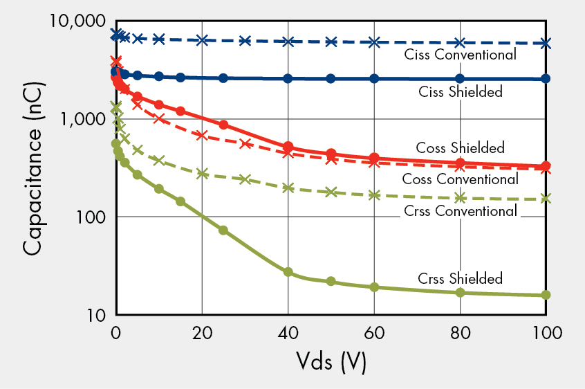
Fig 3 Comparison of Capacitive components for Conventional an Shield Gate Trench with equivalent 20 A RDSon 5.7 mΩ.
Figure 3 compares the capacitive components of the conventional and the shielded gate TRENCH MOSFET having equivalent RDS-on. By reducing the Crss the switching losses are minimized by shortening the time it takes to transition from the off to the on state or the on to the off state. In particular, reducing the Qgd, as show in Figure 4, reduces the switching energy losses by minimizing the time the device has the simultaneous application of high voltage and current.

Fig 4 Comparison of Qg curves at 20 A and 50 V for Conventional an Shield Gate Trench with equivalent 20 A RDSon 5.7 mΩ
Further, the shield and its resistance act as a built in snubbing resistance (Rshield) and capacitance (Cdshield) network depicted as component of the Coss in Figure 3. This snubbing network slows down the transition of the switching from low to high voltage. This feature of the shielded gate helps to reduce EMI, dv/dt induced turn-on, and avalanching during switching transitions.
Performance Improvements in DC-DC 1/16 Brick Module
Fairchild’s FDMS86252 150 V shielded gate MOSFET was compared against competitive MOSFETs in the primary of a 48 V input and 3.3 V output isolated DC-DC converter operating at 400 kHz over the current range of 10 to 20 amps. In Figure 5 the FDMS86252 shows a minimum of 0.4% improvement in efficiency with shielded gate. That translates to at least a 0.32 W power improvement that seems small but is crucial in DC-DC design where every percentage point is crucial when trying to meet regulatory requirements.

Fig 5 Comparison of Fairchild FDMS86252 150 V shielded gate MOSFET against a competitor in a 48 V VIN; 3.3 V VOUT, Isolated DC-DC converter operated at 400 kHz.
Summary
Fairchild’s new PowerTrench MOSFET Technology exhibits better RDSon and Qg improvement compared with previous generations. The technology has enabled the power supply designer to boost efficiency and power density to new levels.
 If you enjoyed this article, you will like the following ones: don't miss them by subscribing to :