Power Tip 41: Powering DDR memory
(Editor’s note: to see a linked list of all entries from #1 to the latest one, click here.)
Power dissipation within CMOS logic systems is primarily related to clock frequency, input capacitance of the various gates within the system, and the supply voltage. As device feature sizes and, hence, supply voltages have been reduced, significant gains have been made in lowering dissipation at the gate level.
These reduced dissipations and higher-speed operation of the lower-voltage devices have allowed system clock frequencies to be pushed up into the gigahertz range. At these very-high clock frequencies, controlled impedances, properly terminated busses and minimal cross-coupling provide a high-fidelity clock signal.
Traditionally, logic systems have been designed to clock data on only one edge of the clock, while the double data rate (DDR) memory clocks on both the leading and falling edge of the clock. This doubles the data through-put while slightly increasing system power dissipation.
The increased data rate requires that the clock-distribution network be carefully designed to minimize ringing and reflections, which may inadvertently clock-logic devices. Two candidate bus-termination schemes are presented in Figure 1.

Figure 1: VTT termination voltages reduce termination power by half.
In the first schematic (A), bus-termination resistors are placed at the end of the distribution network and are connected to ground. If the bus driver is in the low state, the resistors have zero dissipation. In the high state, the resistors dissipate power equal to the supply voltage (VDD) squared, divided by the bus resistance (source impedance plus termination resistor). The average loss is the supply-voltage squared divided by twice the bus resistance.
In the second scheme (B), the termination resistor is connected to a supply voltage (VTT) that is half the VDD voltage. The dissipation in the resistor is then constant, regardless of the supply voltage and equal to VTT (or (Vdd/2)) squared divided by the termination resistance. This results in a factor-of two-power savings when compared with the first approach, but at the cost of needing an additional power supply.
Note that the requirements on this power supply are somewhat unique:
•First, its output needs be half that of the driver voltage (VDD).
•Second, it needs to both source and sink current. When the driver output voltage is low, current flows from the VTT supply. However, when the driver is high, current flows into the supply.
•Third, the supply needs to transition between modes as the system data changes and must provide a low-source impedance, up to near the clock rate of the system.
Peak power is relatively easy to determine from the termination resistors, the clock frequency, and the capacitances within the system. Average power is harder to estimate and can be many times less than one-tenth of the peak power. You need to consider such things as the fact that the system is dynamic and does not really have a fixed clocking rate, data is not clocked every cycle, and there will be devices that are tri-stated. Average current is an important number to verify with system measurements as it can be important for determining the appropriate power supply topology. For example, you would trade the low-power dissipation of a switching power supply against the low cost and size of a linear regulator.
Table 1 shows the comparison in component count, area requirements, dissipation, and cost for a switcher versus a linear regulator. This is for regulators which can output 3A of peak current. It is interesting to note that dissipation is going to be hard to handle, if the peak current is present all the time. Establishing the DC current will drive the choice. Clearly, the linear regulator is favored from all other aspects.
One significant challenge with a DDR power supply is controlling the output voltage during wild transient loading extremes. As shown in the table, the linear approach has a much-wider control bandwidth than the switcher.
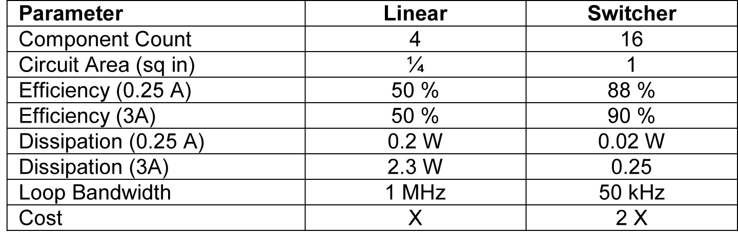
Table 1: Linear approach is smaller and costs less, but is not as efficient as a switcher.
Consequently, it uses much-smaller capacitors to control output impedance. For instance, to control the output to within 40 mV with a 3A load, the output impedance at the crossover frequency needs to be less than 0.013 Ω, which corresponds to about 10 μF of capacitance. A switcher with a linear control loop closed at 50 kHz takes over 200 μF of capacitance, which results in additional cost and circuit board area (see Power Tip #10).
To summarize, DDR memory enhances system speed by clocking data on both edges of the clock, resulting in increased through-put. Termination resistors are required to reduce voltage reflections because of the high frequency operation. Losses in the terminations can be minimized by connecting one end with a voltage equal to half the supply voltage.
This supply needs to be able to source or sink current and must have a high crossover frequency to minimize capacitor requirements. A linear regulator approach for the termination supply can save money and size, if the increased power dissipation is acceptable.
Please join us next month when we will discuss simple FET gate drive circuits.
For more information about this and other power solutions, visit: www.ti.com/power-ca.
About the author
 Robert Kollman is a Senior Applications Manager and Distinguished Member of Technical Staff at Texas Instruments. He has more than 30 years of experience in the power electronics business and has designed magnetics for power electronics ranging from sub-watt to sub-megawatt with operating frequencies into the megahertz range. Robert earned a BSEE from Texas A&M University, and a MSEE from Southern Methodist University.
 If you enjoyed this article, you will like the following ones: don't miss them by subscribing to :