How to get 500W in an eighth-brick converter with GaN, part 2
In part 1 of this series, we discussed the benefits of eGaN FETs, and showed how these translated directly into better efficiency and vastly improved power density via the example of a 500W eighth-brick demonstration converter. This is a 70% increase in power over the best silicon has to offer. We further showed that for an unregulated design, we could achieve an astounding 667W. eGaN FETs are the key to making this possible, but to get this kind of performance, an engineer has to think carefully about the design of the converter. With silicon MOSFETs, the reduced performance of the FETs overshadowed much of these details. However, once the designer dives in and gets into the proper mindset, it will pay many dividends.
In part 2 of this article, we dive into some of the key details of physical and electrical design. We will look at layout, key waveforms, and losses. Along the way, one may notice things that could be improved. We summarize key potential improvements near the end of the article.
Layout
In order to get the maximum benefit from using eGaN FETs, proper attention to layout is crucial. Our approach is to do the entire power stage first, including gate drives and bus caps, and make everything else work around it. This approach is not unique to working with GaN, but the performance compromises with silicon and its complex packaging can obscure much of the benefit of a good layout. The key points in the layout are:
- Minimize power loop inductance to minimize losses and ringing [1].
- Maximize power stage symmetry in order to maximize volt-second balance on the transformer [2].
- Use copper for thermal management wherever it does not compromise electrical performance.
- Do not let power currents flow across signal grounds.
For reference, we show again the simplified schematic of the converter in Figure 1.

Figure 1 Simplified schematic of E-brick converter.
The PCB is implemented with a 12 layer board. The ten inner layers are 4 oz. (140 µm) copper to handle the high currents, and the outer layers are 2 oz. (70 µm) to accommodate the finer pitch of the surface mount components. The board uses 3 types of vias: through vias, buried vias (layers 2-11), and microvias (layers 1-2 and 11-12). All vias are filled and plated to allow via-in-pad design with reliable soldering. The microvias provide a low electrical and thermal resistance for the FETs, and greatly simplify the remaining layout.
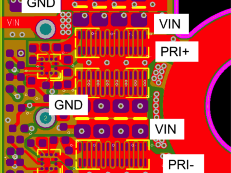
Figure 2 shows a top-down view of the overall layout. We see the full-bridge input on the left, which feeds the integrated planar transformer windings, and finally the synchronous rectifiers (SRs). The snubbers are adjacent to each SR. The controls take most of the remaining space. The bottom side contains the input and output filter inductors, the bias supply, and the signal isolation. Finally, we note the line of symmetry for the power stage. Small variations are acceptable, but this symmetry is important to maintain volt-second balance on the transformer without the need for a blocking capacitor or primary side current sensing.

Figure 2 Overview of converter layout (top view).
Figure 3 to Figure 5 show the details of the primary side power stage layout. The primary side is comprised of two half-bridges, so the EPC’s recommend optimal layout is used, and repeated twice [1]. Figure 3 shows the top layer (L1), including all connections to the FETs, the input bus VIN, the reference bus GND, and the primary winding connections. The low side FETs use microvias to connect to the ground plane on the next layer (L2). Through vias are used to connect the FET connections to multiple internal heavy copper planes to minimize thermal and electrical resistance.

Figure 3 Primary side layout, layer L1 (top layer).
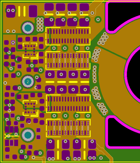
Figure 4 Primary side layout, layer L2, showing ground bus.
Figure 4 shows the second layer from the top (L2). This layer is used for power and signal ground. The microvias from the top (L1) terminate on this layer. In addition, buried vias connect multiple internal ground layers. L2 is not connected to the input ground terminal on this layer, preventing pulsating ground current from flowing across the signal ground plane. This connection is made through multiple internal ground layers that connect to L2 under the FETs and gate drivers. Finally, note that the ground plane is continuous under the power FETs, connecting both half-bridges with a low impedance plane.
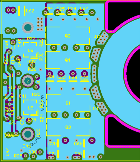
Figure 5 Primary side layout, layer L3, showing VIN bus.
Figure 5 shows L3, which is used to provide VIN for the power stage. It has through vias that allow connection to the top layer and the FETs, as well as connecting to multiple VIN planes to minimize electrical and thermal resistance. As with the GND layer L2, L3 is continuous, connecting both half-bridges with a low impedance plane.
The remaining layers are used to repeat VIN and GND connections, along with some extra copper connecting to the transformer inputs PRI+ and PRI−.

Figure 6 Secondary side layout of one of the two SR switches, layer L1 (top layer).
The other critical part of the power stage layout is the SR. Figure 6 and Figure 7 show one half of the SR and its relationship to the transformer winding. From Figure 6, we see that the transformer winding is enlarged upon leaving the core area and forms the drain terminal for the two parallel eGaN FETs forming the switch. Note that the drain connection has numerous through vias, both at the transformer terminal and interspersed among the two FETs. These allow connection to the four parallel layers forming the transformer secondary. Because of the high currents, it is important to maximize the copper area to reduce electrical and thermal resistance, much more so than on the primary side. Source connections are made using microvias in the source pads of the FETs. This allows an excellent thermal and electrical connection to ground layer L2.

Figure 7 Secondary side layout of one of the two SR switches, layer L2, showing output return layer (VOUT−).
Figure 7 shows the second layer that forms a ground connection underneath the FETs. The microvias connecting from L1 can be seen, as well as the through vias. In addition, we use buried vias to allow connection to the remaining ground layers in the board. The ground layer extends to the FETs in the other SR switch to minimize the inductance of the loop formed by the source of the two SRs. The ground layer also extends to the right and forms the return path for the gate drivers, as well as extending further to the right to form the signal ground for the controller and sensing circuitry (not shown). In a manner similar to the primary side, this ground layer does not connect to the converter output terminal (VOUT−) to prevent the high output ground currents from flowing across the signal ground.
Electrical performance
Finally, let’s take a look at the converter waveforms (Figure 8). These waveforms are taken at full load (42A) with a nominal input of 52V. First, we consider the primary gate drive waveform, shown in dark blue, along with the corresponding primary switch node waveform. The voltage fall time is about 10 ns. Note the extremely clean waveforms made possible via the low eGaN FET inductance and careful layout. The ringing on the primary waveform is due to the transformer leakage resonance with the FET capacitance, but does not stress the device. When the primary transistors are turned on, there is no ringing, which suggests that the gate resistance could be reduced for even faster switching and better efficiency.

Figure 8 Converter waveforms with 52VIN and 42A load. Turn-on is shown at right and turn-off at left. The time scale is 50 ns/div.
Next, let’s examine the drain voltage of one of the SRs. A look at deadtime conduction through the body diode reveals the short period of time at each transition where the body diode conducts briefly while the channel is turned off. At this time, the SR drain voltage becomes negative for a deadtime of approximately 25 ns. The reverse voltage drop is higher on the left-hand side because at the beginning of the primary off-time, only one SR is conducting, and it takes time for the current to split evenly between the SRs. On the right-hand waveform, both SRs are conducting during deadtime, hence the voltage drop during deadtime is smaller for this interval.
SR deadtime conduction loss can be estimated [3] and accounts for an estimated 1.3W loss at full load. The controller is capable of 1 ns resolution, so it is possible to shorten deadtime at full load, and increase full load efficiency by 0.1 to 0.2%. The challenge arises because the controller code implements fixed delay times for the deadtime control, referenced to the primary switching waveforms. At light load, the reduced dv/dt means longer transition times and this results in a smaller deadtime. An adaptive deadtime in the control would be a promising option to further improve efficiency.
Adaptive deadtime is much more difficult to implement with silicon MOSFETs. The primary difficulty is reverse recovery of the MOSFET body diode. Reverse conduction through the body diode is a practical requirement for soft commutation. While the voltage drop may be less, this reverse current results in reverse recovery, meaning that the diode doesn’t turn off for some period after the primary switch turns on, essentially resulting in a shoot-through current and high losses. This can be mitigated with adaptive deadtime as well, but is very challenging. This is because reverse recovery is difficult to accurately characterize, and is a strong and highly nonlinear function of reverse current, temperature, and deadtime. It gets much worse with temperature. As mentioned in part 1, it is effectively an unpredictable moving target. Even if one could optimize it, the huge gate capacitance of silicon MOSFETs typically used in SRs results in slow switching speeds. This means that even an optimized design with silicon can only minimize the effects of reverse recovery, but not eliminate them. On the other hand, eGaN FETs have no reverse recovery, so these problems go away. The timing is controlled, repeatable, and varied little with temperature, hence adaptive deadtime should be much simpler to realize.
Finally, we examine the SR drain waveform as it is driven off the primary switch. We see a narrow initial spike which the snubber does not completely capture due to the inductance of the snubber network, estimated at 2 nH. Under the test conditions shown, this spike reaches 36V, and is 5 ns at its base. At the end of the initial spike, the snubber diode conducts and stores the leakage energy on a cap, and after a short delay, this energy is returned to the output inductor through the winding (not shown). With a 60V input, this spike reaches an amplitude of about 42V, so 60V FETs were chosen. A lower inductance snubber loop could be used to reduce the spike amplitude and permit the use of 40V FETs for the SRs, which would lead to an efficiency improvement.
Losses
In Figure 9, we take a look at the loss breakdown of the converter. This chart is the result of both analysis and simulation results and assumes a uniform temperature of 100°C, with a total estimated loss of 16.6W. It does not include vias, solder joints, and traces outside the transformer windings.

Figure 9 Estimated loss breakdown at 100°C, with a total estimated loss of 16.6W.
Nearly 50% of the losses are due to magnetics. The actual breakdown in operation has lower output inductor loss and higher transformer loss, since the transformer windings are hotter than 100°C while the inductor is substantially cooler. However, this doesn’t change the fact that the magnetics loss dominates the total losses. Other losses include bias supply, controller, sensing, gate drive, and other miscellaneous power, accounting for about 25% the total loss, the majority of which is the bias supply losses, followed by the controller. The combined switching and conduction loss in the FETs is only approximately 25% of the total loss.
Potential improvements
Although eGaN FETs already demonstrate a tremendous leap in performance, there is still room for improvement summarized here:
- Optimize the bias supply: This supply is over-sized since it was adopted from a silicon MOSFET-based design. Due to the minimal gate power requirements of the eGaN FETs, a savings of at least 0.5W, or about 0.1% added full-load efficiency (more at light load) could be realized.
- Add heat sinks to the transistors and transformer core.
- Optimize the gate resistors: This would result in even faster switching speed.
- Adaptive deadtime: This would minimize diode conduction for an additional 0.2% efficiency at full load (a savings of up to 1W).
- Custom magnetics: This could reduce transformer and inductor losses, especially transformer core loss.
- Revisit the switching frequency and adjust for maximum performance.
These changes could result in at least another 0.3% improvement in efficiency at full load, and likely more, pushing the performance of the fully regulated converter over 97%.
Summary
In part 1 of this series, we explained why eGaN FETs are able to open the door to dramatic improvements in efficiency and power density due to performance superior to silicon MOSFETs, and went on to show that the benefit is real with the design of a 500W eighth-brick demonstration converter, a 70% increase in power compared to the best available design based on silicon MOSFETs. Furthermore, we did this with a conventional, fully regulated, hard switched design. We’ve also shown that unregulated hard-switched designs can be pushed over 650W.
While eGaN FETs can be used in the same applications as MOSFETs, to get the maximum benefit, careful attention must be paid to the layout and design. This article illustrates our approach to save design engineers time and effort. After a discussion of layout best practices, we looked at some waveforms, which showed the benefits of the layout, and showed places where performance could be further improved. This was followed by a brief discussion of losses, and we wrapped things up with a list of potential improvements to boost performance further. For more detail, the full schematic, BOM, and Gerber files are freely available on EPC’s website [4, 5].
The benefits of GaN technology go well beyond this one example. A more in-depth exploration on the use and benefits of GaN in DC-DC applications, including practical details on layout and thermal management, as well as its impact on systems and power architectures, is available in EPC’s DC-DC Conversion Handbook: A Supplement to GaN Transistors for Efficient Power Conversion [6].
References
- D. Reusch and J. Strydom, “Understanding the Effect of PCB Layout on Circuit Performance in a High Frequency Gallium Nitride Based Point of Load Converter,” Applied Power Electronics Conference and Exposition (APEC), pp.649-655, 2013.
- R. Miftakhutdinov, “Improving System Efficiency with a New Intermediate-Bus Architecture,” Texas Instruments Inc. Seminar, 2009.
- A. Lidow, J. Strydom, M. de Rooij, D. Reusch, “GaN Transistors for Efficient Power Conversion,” Second Edition, Wiley, 2014.
- “Demonstration Board EPC9115 Quick Start Guide,” Efficient Power Conversion Corp., March 2015.
- Schematic, BOM, and Gerber files, EPC
- D. Reusch and J. Glaser, DC-DC Conversion Handbook: A Supplement to GaN Transistors for Efficient Power Conversion, Efficient Power Publications, 1st Edition, 2015.
Also see:
- How to get 500W in an eighth-brick converter with GaN, part 1
- Efficient Power Conversion’s DC-DC Converter Handbook: Power Architectures
- DC-DC Converter Handbook: The latest design insights using GaN transistors
 If you enjoyed this article, you will like the following ones: don't miss them by subscribing to :