High efficiency resonant mode implementation using digital control
The LLC resonant power stage has become an extremely popular power topology in the industry for high power applications that require an efficient power conversion up to and around a kilowatt. Resonant mode is a best fit choice as the second stage of the AC-DC converter as it is typically preceded by the boost Power Factor Correction (PFC) stage that provides a stable high voltage input.
In traditional Pulse Width Modulation (PWM) duty cycle controlled power converters the switching frequency is fixed while the duty cycle varies to maintain a regulated output voltage. In resonant power conversion the opposite occurs – duty cycle is fixed to 50% (minus deadtime) the frequency is allowed to vary.
Some of the advantages of the series resonant converter are:
- High efficiency
- ZVS/ZCS (Zero Voltage/current switching) of primary/secondary switches (depending upon operating mode)
- Increased power density
- Low noise and EMI due to ZCS
- No transformer saturation due to DC current block by resonant capacitor
- Good cross regulation between multiple outputs
- Flatter efficiency curve across the load range
However, there are some drawbacks that complicate the operation of the converter are:
- Soft start and light load operation
- Synchronous rectification drive
- Short circuit behavior
- Difficult to design under a wide input operating range.
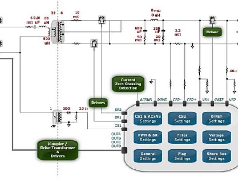
This article shows how the digital implementation of the resonant topology using an advanced digital controller (see Figure 1) makes the control, design, and optimization an easy task and solves the common problems described above. The topology under consideration is the half bridge LLC resonant converter with MOSFETs as switches. However, the same concepts apply to the full bridge SRC (Series Resonant Converter) or even the LCC resonant topology.
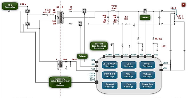
Figure 1. Simplified half bridge LLC power stage
Resonant mode basics
Resonance can be defined as the excitation (or stimulus) that provides a maximum transfer of energy from one part (or element) of the system to another. In an ideal (lossless) system, this transfer of energy can continue indefinitely. Resonance occurs in several places in nature and such as electrical, mechanical, acoustical etc.
Figure 2 to Figure 5 show an LCR circuit operating above and below resonance. It can be seen that only when the operating frequency is at resonance we can get maximum current flowing in the circuit. Another observation is when the excitation frequency (fS) is greater than the resonant frequency (fRES) the input current lags the input square voltage waveform which can be approximated by its first harmonic or fundamental by a sine. The reverse happens when fS < fRES , and the voltages and currents are in phase when fS= fRES. Due to the nature of the plots, we can conclude that when fS > fRES the voltage drops to zero before the current waveform then we can achieve ZVS turn-on of a switch (see Figure 6). The opposite is true for fS < fRES.
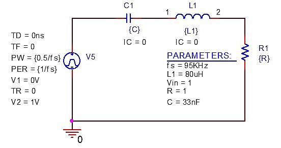
Figure 2. LCR resonant circuit

Figure 3. LCR resonant circuit excited at f= 95KHz< fRES
Red trace: Excitation voltage
Green trace: Current waveform
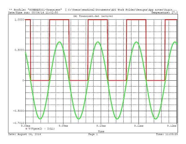
Figure 4. LCR resonant circuit excited at f= 97.95KHz= fRES
Red trace: Excitation voltage
Green trace: Current waveform

Figure 5. LCR resonant circuit excited at f= 100KHz> fRES
Red trace: Excitation voltage
Green trace: Current waveform

Figure 6. Primary side voltage and current waveforms showing ZVS turn on of a switch
Now consider operation in terms of the impedance of the circuit (Figure 7). The input square wave voltage is approximated by its first harmonic – a sine wave of the same frequency. Starting from a frequency below the resonant frequency, we can see that as the frequency increases, the impedance decreases until it reaches resonance. At this point the capacitive and inductive impedances cancel each other out and the impedance turns into a resistance (frequency independent impedance). At this static frequency, from the phasor point of view, the capacitive impedance XC has an angle of -90° whereas inductive impedance XL has an angle +90° . Beyond this frequency the impedance increases further. Hence, the behavior of the circuit can be summarized as follows: from low to high frequency the circuit behaves capacitively (f < fRES), resistively (f= fRES), an inductively (f> fRES).
Therefore, to transfer energy we need to operate in a zone that is close to the resonant frequency otherwise the capacitive and inductive impedances will dominate. By understanding the impedance plot we can conclude that to operate at a lower load we must increase fs and vice versa. This essentially determines the control law.

Figure 7. Input impedance of for Figure 8 at light
load and heavy load
x axis – Frequency
y axis – Input Impedance in dB
Resonant mode basics
Finally, consider the gain curves of the Half bridge LLC converter as seen in Figure 8 and Figure 9 where the gain of the converter increases as frequency decreases (load increases).
The best theoretical operating point is at resonance where the currents are sinusoidal. The advantage of this that due to the alternating currents the switches on the primary side can achieve Zero Voltage Switching (ZVS) during the turn on and the secondary rectifiers can achieve Zero Current Switching (ZCS). However, due to practical considerations such as variation of inductance and input voltage, the operating point is chosen to be slightly lower than fRES and it still enables ZVS and ZCS for the primary and secondary switches respectively. This also allows enough gain to maintain regulation of the output during a dip in the input voltage.
Figure 8. Equivalent Spice circuit of Half bridge LLC converter to derive gain curves
Challenges with resonant mode
While resonant mode provides many advantages, there are challenges to implementation such as soft start behavior, light load operation, short circuit and implementation of robust protection. Here, we show how these issues can be resolved by new techniques implemented in an advanced digital controller.
Soft start
The two main criteria during soft start are to avoid an inrush current and prevent any overshoot in the output voltage. To accomplish this, the digital controller must start off with a high switching frequency and reduce the frequency at a controlled rate which is determined by the speed of the soft start ramp.
This is equivalent to reducing the impedance of the resonant tank circuit at a steady rate that allows a transfer of energy to the secondary side smoothly. Failure to do so will cause the output voltage to rise abruptly causing an overvoltage condition. For a constant load, this is also equivalent to increasing the gain of the circuit as seen from the gain curves. The above mentioned operation is shown in Figure 9 and Figure 10.

Figure 9. Gain curves for the half bridge LLC converter
for fixed Lm and Lres. Plotting increasing values of Rload
x axis – Frequency (Hz)
y axis – Gain divided by transformer turns ratio (reflected to secondary side)

Figure 10. Soft start waveform at 300W, 20ms/div
Yellow trace – primary current, 5A/div
Green trace – Output voltage, 48V output, 10V/div
Red trace – Input voltage (385V), 100V/div
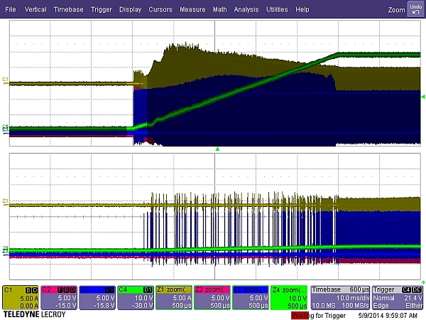
Figure 11. Soft start waveform showing frequency sweep from burst mode to steady state operation at 300W, 10ms/div
Yellow trace – primary current, 5A/div
Green trace – Output voltage, 48V output, 10V/div
blue trace – gate-Source voltage of high side MOSFET, 5V/div
No load and light load operation
From the gain curves (and also the impedance vs frequency plot of the resonant tank circuit), it is evident that as the load decreases, the switching frequency increases to maintain a regulated output. This change in frequency from nominal load to no load can vary by an order in magnitude depending on the ratio of magnetizing inductance (LMAG) to resonant inductor (LRES). Given a typical switching frequency of 100-200KHz, operating the converter at 1 MHz is not a viable option. There is also a constraint in the ZVS condition of the primary switches as ZVS is typically lost at lighter loads. Due to the switching losses it is important to implement a mode similar to pulse skip of duty cycle controlled converters. This is where the burst mode operation would is useful in the digital controller. The user can simply select two thresholds – a maximum frequency and a frequency at which the controller enters/exits burst mode from a drop down list in from the programmable options in the Graphic User Interface (GUI) for the digital controller.

Figure 12. Maximum frequency programming options
Maintaining operation in ZVS region
Resonant topologies can operate in ZVS mode or ZCS mode depending upon the operating switching frequency and its position relative with respect to the resonant frequency (fRES) set by the LRES and CRES. Two conditions demand a decrease in switching frequency (i) increase in load (ii) or decrease in input voltage. However, care must be taken as if the switching frequency decreases by a large amount, the operation of the converter will be in the ZCS region (see Figure 9) where the switching losses become prevalent and there may be cases where the primary MOSFETs fail as the reverse recovery of the body diodes are poor. Also the ZCS condition of the secondary rectifiers is also lost and there may be excessive voltage spikes greater than the breakdown voltage of the secondary MOSFETs.
The advanced digital controller has a programmable threshold on the lowest frequency. This way the user can prevent the converter from entering a region that is deep in the ZCS region. Typically, resonant converters operate with a fixed input voltage. For example, following a boosted PFC circuit. However, the resonant converter should be able to withstand a short amount of time in the ZCS region when the PFC bulk voltage drops off due to a temporary brown out condition.
Short circuit behavior and other protections
There are at least three forms of protection for short circuit behavior that the advanced digital controller can support.
The primary current is sensed using a current transformer (CT) that transfers the primary current information to the secondary. A fast comparator compares this to a threshold to provide a cycle-by-cycle current limit.

Figure 13. Fast overcurrent protection, 100µs/div
Blue trace – Primary PWM, 5V/div
Green trace – Output voltage, 48V output,10V/div
Red trace – Output current,20A/div
The secondary current is sensed using a sense resistor and fed into an ADC. A digital comparator then provides a comparison against a user programmable threshold to set an OCP (over current protection) flag.

Figure 14. Output overcurrent protection after 5ms
debounce time, 2ms/div
Blue trace – Primary PWM, 5V/div
Green trace – Output voltage, 48V output, 10V/div
Yellow trace – Load current, 5A/div
Additionally, for redundant protection there is a general purpose input pin called FLAGIN that trips fault based on a binary input (active high). An external comparator can be used to signal the controller during a surge in current due to a short circuit.
PWM setup and synchronous rectification for resonant mode
The PWM for the primary switches is simple and consists of setting the deadtime between the falling edge of the switch that turns off and the rising edge of the switch that turns on. Deadtimes can be adjusted in steps of 5ns by a simple dragging and dropping the PWM edges via the GUI.

Figure 15. Example of PWM deadtimes in the GUI.

Figure 16. Example of ZVS turn on of primary switch, 200ns/div
Blue trace – Drain voltage, 100V/div
Yellow trace – PWM gate signal, 5V/div
The driving of the synchronous rectifiers (SR) is also done in a similar manner. A simple and effective technique is to use a reference signal that is available in the circuit itself. The reference point is taken from the drain of the secondary rectifier. Since the voltage across the transformer is a square wave the reflected voltage on the secondary is also a square wave. This signal can be used as the reference to turn on the SR PWMs. Setting the SR1 and SR2 PWMs is done in a similar fashion to the primary PWMs i.e. adjusting the deadtimes. There are 2 independent controls for each synchronous rectifier that can be adjusted to set the deadtime as shown in Figure 17.

Figure 17. Synchronous rectifier PWM timing with ACSNS reference
Advantages of this method are that it does not rely on an external gate driver. When several switches are paralleled to reduce the Rdson parameter there can be a difficulty in detecting the on voltage across the switch which may not turn. This method operates over the entire frequency range (fS> fRES and fS<fRES) and allows ZCS turn-on of the secondary switches after the Qrr transition has taken place with the help of the adjusted dead-time feature. This allows a completely snubber-less design to be implemented. Using the fine deadtime adjustment the reverse recovery current that varies from the choice of MOSFET used can be prevented (see Figure 18 and Figure 19).

Figure 18. Example of improper deadtime causing reverse current to shutdown power supply due to primary overcurrent protection.
Pink trace – Primary current
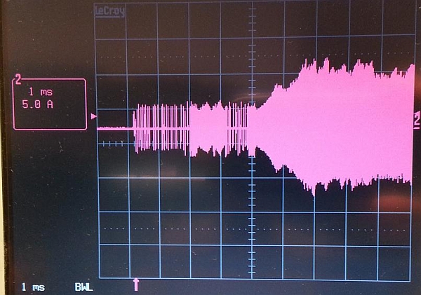
Figure 19. Example of proper deadtime preventing reverse current to shutdown power supply due to primary overcurrent protection. Converter starts and operates at normal load.
Pink trace – Primary current
Alternately, to implement use the synchronous rectifiers during the soft start process, two of PWMs with configurable deadtimes can be used to drive the rectifiers. This is done so because the on time of SR1 and SR2 is a subset of the primary PWMs. Hence, the SRs can be activated during the complete soft start process.

Figure 20. Synchronous rectifier INCORRECT timing, 1µs/div
Yellow trace – primary current, 1A/div
Red trace – secondary current, 2A/div
Blue trace – SR PWM, 10V/div
Green trace – 48V output voltage, 10V/div

Figure 21. Synchronous rectifier CORRECT timing, 200ns/div
Yellow trace – primary current, 2/div
Red trace – secondary current, 5A/div
Blue and green trace – SR PWM, 5V/div

Figure 22. Synchronous rectifier snubberless turn off, 200ns/div
No ringing observed on SR drain
Yellow and red trace – SR drain, 50V/div
Green and blue trace – PWMs, 5V/div
Additional requirements for digital control
Frequency resolution and limit cycling
Due to the quantized nature of the output voltage by the use of an Analog-Digital converter (ADC), the error signal is also discretized. This means that the error signal must fall in a zero error bin when the output voltage is in regulation. This is achieved by using a fine PWM resolution in duty cycle controlled converters. The counterpart to digital pulse width modulation resolution (DPWM) is frequency resolution and the criterion to be satisfied is:
![]()
where qA/D is the quantized LSB of the ADC sensing the output voltage, HTANK(S) is the transfer function of the resonant stage, HSENSOR is the gain of the feedback network, and is the frequency resolution. The above equation only states that the frequency resolution must be fine enough to put the output voltage within less than an LSB of the quantized output voltage after taking into account the sensor gain (the feedback divider ratio). This fine resolution prevents the control loop from bouncing the output voltage about the steady state voltage identified by the zero error bin. This is known as the limit cycling behavior.
Extremely fine resolutions are possible as long as the trade off as long as the digital clock speed does not result in an excess power consumption of the digital core. The update rate of the switching frequency must be equal to fRES at a minimum. An update rate at a lower frequency creates a phase lag in the overall loop gain of the system and large signal disturbances such as dynamic load step will yield a poor performance. An update rate of 4 times fRES is typical as it updates the switching frequency at the maximum, minimum and zero crossing points of the primary current waveform. Such an update rate does not pose any danger of saturating the transformer from a DC bias due to the CRES which also acts as a blocking capacitor.
Compensation of the resonant mode converter using the digital controller
Figure 1 introduces the ADP1046A– an advanced digital DC-DC controller with used in a typical resonant mode application. The ADP1046A has a state machine based approach and includes several other features such as redundant OVP, over current protection for primary and secondary sides, first flag ID that identifies the first instance of failure, and telemetry. It also has an intuitive GUI that eliminates any form of software programming. It has a frequency resolution of 10ns. This means that the frequencies about a nominal frequency of 150KHz will be 149.775KHz and 150.225KHz.
Figure 23 shows the digital compensator window of the ADP1046A GUI. The ADP1046A uses a Type III PID compensator to compensate the plant. Although the compensator is implemented in the z domain, the GUI uses the Bilinear Transformation to display the Bode plot in the s domain. This, along with a state machine design methodology allows the power designer to avoid designing the compensator in the z domain and work directly in the s domain. The LC filter stage, digital filter stage, and loop gain are displayed. The GUI also takes into account the damping effect of parasitic resistance.
Changing parameters such as increasing the low or high frequency gain, location of zeros etc. can be done in a graphical manner. Fine tuning the loop gain and the response to a step load can be optimized on-the-fly for various loads while the power supply is running a dynamic load test. Separate digital compensators for heavy load and light load mode are available.

Figure 23. Filter window in the ADP1046A GUI.
Conclusion
This article introduces the resonant mode topology and offers some brief insight into its operation. It also demonstrates some of the advantages that advanced digital control techniques can bring to resonant conversion by resolving traditional challenges such as soft-start, short circuit protection and synchronous rectification control. Fine deadtime adjustment of the synchronous rectifier PWMs prevents any voltage spikes and offer a snubberless solution.
Using the state machine approach of an advanced digital controller such as the ADP1046A along with the GUI, the power engineer can easily transition to a digitally implemented solution for resonant topologies. Loop compensation is also easily achieved without any knowledge of inverse z transforms. The GUI provides easy configuration of the extensive protection features inherent to the controller, offers debugging tools and telemetry.
About the author
Subodh Madiwale works as an Applications Engineer for Analog Devices in the Digital Power Management group since 2010. Formerly, he held a position at Power Integrations as an FAE designing power supplies. His interests range from system modeling and design, high frequency power conversion and control to mixed signal SOC.
 If you enjoyed this article, you will like the following ones: don't miss them by subscribing to :