GaN single chip integrates sensors for the first time
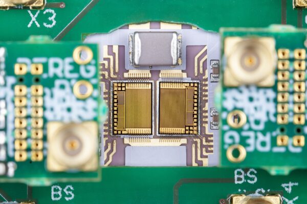
For the GaN single chip, the team at Fraunhofer Institute for Applied Solid State Physics IAF in Freiburg combined current and temperature sensors, 600V power transistors with intrinsic flyback diodes and gate drivers.
Compared to conventional voltage converters, the new circuit not only enables higher switching frequencies and thus a higher power density, but at the same time fast and accurate condition monitoring directly in the chip. This is important because the increased switching frequency of GaN-based power electronics enables very compact designs, but also leads to stricter requirements with regard to monitoring and control. “Therefore, sensor technology integrated in the chip is a great advantage,” said Stefan Mönch, researcher at Fraunhofer IAF and part of the GaNIAL research project.
The integrated current sensor now enables the non-reactive measurement of the transistor current for control and short-circuit protection and saves space compared to conventional external current sensors. The integrated temperature sensor enables direct measurement of the temperature of the power transistor and thus maps this thermally critical point much more accurately and quickly than previous external sensors, as the distance and resulting temperature difference between sensor and measuring point is eliminated by the monolithic integration.
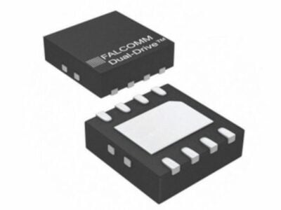
“The monolithically integrated GaN power electronics with sensor technology and control thus saves chip space, reduces the effort required for assembly technology and increases reliability. This is crucial for applications in which many small and efficient systems have to be installed in a small space, such as electromobility,” said Mönch, who designed the 4 x 3 mm² GaN chip.
The GaN single chip is built on a silicon substrate (GaN-on-Si) using lateral devices. This allows the current flows parallel to the chip surface so that all connections are located on the top of the chip and connected via conductor paths. This lateral structure of the GaN components allows the monolithic integration of several components such as transistors, drivers, diodes and sensors. This then allows the higher switching frequencies and a higher power densityi n power converters as well as fast and accurate condition monitoring within the chip itself. “Although the increased switching frequency of GaN-based power electronics allows for increasingly compact designs, this results in a greater requirement for their monitoring and control. This means that having sensors integrated within the same chip is a considerable advantage,” said Mönch.
Related GaN single chip articles:
- DRIVING GAN TECHNOLOGY INTO AUTOMOTIVE DESIGNS
- PANASONIC BOOSTS GAN TECHNOLOGY WITH INTEGRATED POWER SWITCH
- SINGLE CHIP GAN HALF BRIDGE CONVERTS 12V TO 1.8V AT 5MHz
- SO WHERE IS THIS POWER REVOLUTION THEN?
 If you enjoyed this article, you will like the following ones: don't miss them by subscribing to :