Step by step for an optimised flyback design: Isolated close loop design – Part 2
This article is the second part of a two-part series. To read part 1 of the series click here.
The control close loop modelling and compensation stage of an isolated flyback power supply has always been considered the most challenging part of the design, with complicated AC modelling, and obscure compensation rules. Designers tend to avoid the pure academic mathematic approach to the problem and rely more on practical lab test results, like load and line transient response, or the switching waveform of the switching node of the converter.
This article demystifies close loop modelling of a flyback design with a simple mathematic approach, guiding the designer to a well-optimised design.
Close loop design
The best design approach is to have a simple and intuitive model of the control circuit, select the proper compensation network, and verify the results with a more precise close loop measurement with the network analyser. Following it is a description of a crude method that provides a good understanding of the problematic nature of the flyback close loop analysis with PWM peak current mode control, operating in continuous conduction mode.
At the beginning of a switching period (T), the switch is turned on, and the inductor current is sensed by Rsense and the current-sense amplifier. This current-sense signal is added to a corrective ramp, and when the sum of these two waveforms exceeds Vc, the comparator output goes low, turning off the output switch.
The power supply system can be represented by the simplified model in Figure 1:
- Control-to-output stage that includes the modulator, transformer, and output filter
- Compensation stage of the error amplifier, that is designed in order to make the power supply stable

PWM peak current mode control
The control to output transfer function can be simplified as one low frequency pole, one zero, the right half plane zero already mentioned before, and the two sampling poles associated with any current mode control:
Single low frequency pole given by the output capacitor (Co) and the output load (Ro):

Where D is the duty cycle.
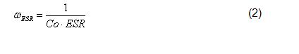
The additional zero given by the output capacitor (it’s capacitance and ESR value) is:
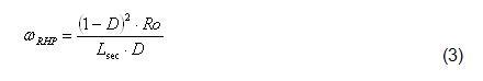
The dependency of the RHP zero location ωRHP versus primary and secondary inductance Lsec of the transformer was explained in more detail in the previous article regarding flyback power supply optimization; below the RHP is expressed in rad/sec:
The right half plane zero has the same 20 dB/decade rising gain magnitude as a conventional zero, but with 90° phase lag instead of lead, this characteristic makes it difficult to compensate the RHP zero. RHP zero occurs only in boost and flyback topologies.
The practical effect of the RHP zero is shown in Figure 2: with a temporary increase of the duty cycle corresponding to a decrease of the conduction time of the diode, which translates into a decrease of the average diode current (the output load current).
This undesirable effect of the RHP zero is not seen when the converter operates in discontinuous conduction mode because an increase of duty cycle does not influence the conduction time of the diode, since both primary and secondary inductors are completely discharged each cycle, and the current is able to ramp up to full load each time.

decrease of the average current to the load
An important property of peak-current-mode control is the sampling effect:
this phenomenon, which is intrinsic in all peak-based current controls, introduces in the control to output transfer function a couple of poles at half the switching frequency fsw/2 with a quality factor Qsp depending on duty cycle D, and ratio between the inductor current ramp slope Sn and the compensation ramp slope Se.

Where Rsense is the current sense resistor in series with the switching MOSFET to sense the peak primary current of the transformer.
For duty cycle greater than 50%, current mode control loops are subjected to sub-harmonic oscillation. This instability can be eliminated by adding an additional fixed slope voltage ramp Vslope signal to the current sense signal Sn. This technique is commonly known as “slope compensation”.
Typically all the peak current mode controllers already have a fixed internal slope compensation that can be increased by increasing the source impedance of the current sense signal.
Then the overall transfer function of the power stage is obtained:

Where ADC is the DC gain of the power stage:

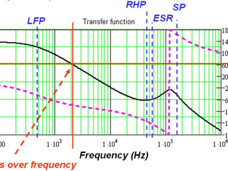
Figure 3 shows the typical gain and phase of the overall transfer function over frequency. This approximated plot can be used to understand how to design the control/compensation circuitry and therefore improve the stability and dynamic of design.
In practice, when there is the possibility to make a real AC loop measurement of the power stage it’s advisable to obtain real plots with a network analyser, and study the compensation network from real measurements.

Figure 3: Gain and phase plots of the open loop power stage transfer function
Error amplifier compensation technique:
The purpose of adding compensation to the error amplifier is to counteract some of the gains and phases contained in the control to output transfer function that could jeopardise the stability of the power supply. Obviously, the ultimate goal is to make the overall closed loop transfer function satisfy the stability criteria.
Thus compensation network transfer function is added to the control output transfer function in order to meet the static and dynamic performance requirements while maintaining stability.
In theory an ideal loop gain should have the following attributes:
– Fast loop response, achieved by a high bandwidth (high cross zero frequency)
– Loop gain slope of 20 dB/decade from low frequency to half the switching frequency
– High DC regulation accuracy in order to have small DC voltage changes with load and line variations, obtained with a large DC gain
– Good noise immunity, with low gain at high frequency close to the switching frequency.
– Flat phase curve near crossover frequency
– Good phase margin in order to have stability with minimum overshoot
The DC gain is the gain at low frequency, crossover frequency is the frequency where the gain cross the line of 0 dB, and phase margin is the difference between the total phase shift measured at the cross zero frequency and 180.
In order to have a high bandwidth while limiting the gain at high frequency, for a flyback the crossover frequency should be limited to one forth below the right-half-plane zero
A pole in the origin of the compensator gain is included to guarantee nominal zero steady state error of the output voltage.
The location of zeros and poles of error amplifier gain can be easily determined using the “K factor” method.
K factor method is based on a simple concept. Given the desired crossover frequency fc and the required phase margin øfc initial phase margin of uncompensated loop gain ømu at that frequency fc allows the designer to calculate the phase boost phb that compensator gain must provide at crossover frequency:
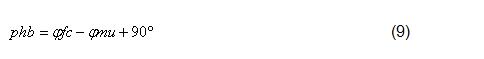
The “+90° additional phase boost is required to compensate for -90° phase shift of the pole in the origin.
Typically a flyback power supply with peak current mode control has a phase boost between 0< phb <70°where a type two compensation is sufficient to provide the required phase boost.
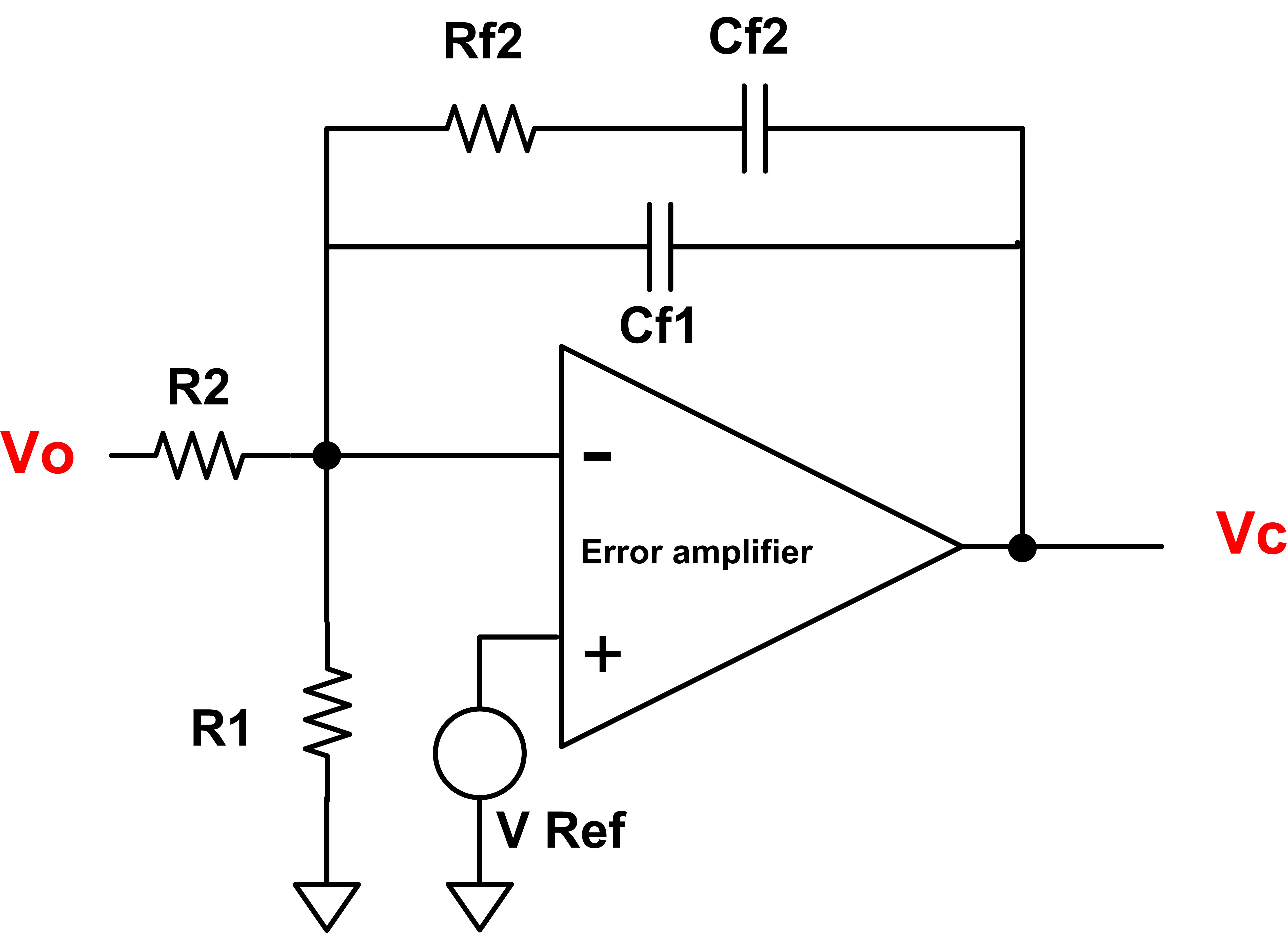
The type two compensation network of figure 4 has one zero and one pole located respectively at: ωz1 = fc/K and ωp1 = fc.K, where K = tan(phb/2+45°)
The transfer function of the compensation stage Berror(s) if it’s ignored the effect of the real operation amplifier is:
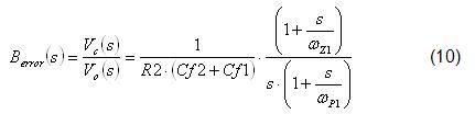
The overall close loop transfer function is obtained multiplying the above compensation stage transfer function (equation 10) with the control to output transfer function of the power stage (equation 7).
How to cross the isolation boundary
One of the main advantages of the flyback converter or any other transformer type converter is the possibility to create one or more outputs with return ground isolated respect the input power ground.
In large systems with multiple power rails, isolation between grounds eases single point grounding, preventing ground loops. Often the isolation requirement is specified from various safety agencies.
The main challenge on the power supply designer is to transmit the output voltage information or error signal information from one ground reference to the other ground, as shown on Figure 5.

Figure 5: Top: Isolation of the output signal, bottom isolation of the error signal
The feedback signal that is returned across the boundary can be a signal proportional to the output (Figure 5 top), or a signal proportional to the difference between the output voltage and a reference voltage (Figure 5 bottom).
Usually is preferable to return back through the isolation barrier the error signal, due to the fact that if you attempt to bring the output voltage directly across the boundary, any accuracy caused by the isolation circuit will directly affect the regulation.
A typical implementation of the isolation of the error is shown in Figure 6: an external operation amplifier like an LMV431 or something similar with type two compensation network is used to create the error signal that pass the isolation boundary through of the opto-coupler. RC2 and Cc are the external network connected to the output of the opto-coupler to help with the stabilization. CRT is the current transfer ratio Ic(s)/Id(s) of the opto-coupler.

The additional transfer function of the opto-isolation network (error amplifier output to modulator input) is:
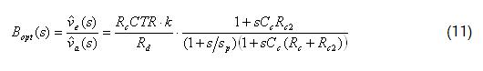
The opto pole location sp depends on the opto-circuit configuration (common emitter in this case), and can be determined from knowledge of the small signal internal resistances and capacitances of the opto-coupler.
The overall feedback transfer function is the compensation network (equation 10) previously discussed multiplied by opto-network transfer function (equation 11).
The above explained method, to model the overall compensation network, with isolation and without isolation, does not take in account the not ideality of the error operation amplifier. The non ideal frequency response of the operation amplifier could lead to over estimating the phase margin and the DC gain of the overall system. Therefore it’s always preferable do not rely only on the mathematic modeling but optimise the compensation network values with a more accurate laboratory measurements of the overall system.
Typical isolated DC-DC converter design for Power over Ethernet power supplies
Figure 7 illustrates a typical PoE application circuit with the LM5072, National Semiconductor’s integrated 100V PoE PD interface and PWM controller with auxiliary support. The LM5072 provides the flexibility for the PD to also accept power from auxiliary sources such as AC adapters in a variety of configurations.

High integration level of the LM5072 controller enhances IEEE802.3af compliance design with minimum number of external components.
How to measure the close loop with a network analyser
Beside the fact, that mathematical models of switching power supplies are getting better, they still have some limitations about the accuracy. The main reasons for those limitations are unknown details about the system. For example: component parasitics, PCB layout, temperature effects, propagation delays, non linearity’s of all semiconductors. A real measurement almost always differs from the mathematical prediction and the efforts to get good models can be extremely high and time consuming. Therefore, it’s always a good idea to actually measure the transfer function. Of course a mathematic model is very useful to calculate the compensation network (R-C values) before one actually build it and then cross check by doing a real loop measurement and do a fine tune. Just to clarify, it’s not a question of whether to use a mathematical model OR a real loop stability measurement. An expert in power supply designs will always do both.
The method explained above is applicable for any switching power supplies regardless the topology or PWM control scheme.
It is important to note that for a stable loop, negative feedback must be used. The response of the loop will opposes any change at the output. This means that if the output voltage tries to rise (or fall), the loop will respond to force it back to the nominal value. If a sinusoidal waveform (or noise) is injected into the loop, the signal will go through the loop and it will come back multiplied by the loop gain with a certain lag phase respect to the injected signal. The phase shift is defined as the total amount of phase lag, referred to the starting point of -180° (negative feedback loop) that is introduced into the feedback signal as it goes around the loop. The loop gain is defined as the ratio of the amplitude of the signal that goes through the loop divided by the amplitude of the injected signal: Loop Gain [dB] = 20*log (Va/Vb)
Let’s assume we inject a sinusoidal signal into the loop across a wide frequency range. At low frequencies, the signal comes back with a larger amplitude and at high frequencies it is attenuated. All measured values, the gain and the phase, will be recorded. The result of the measurement is the so called bode plot (see example in Figure 8). The graphs say a lot about the loop stability and certain points are of special interest.
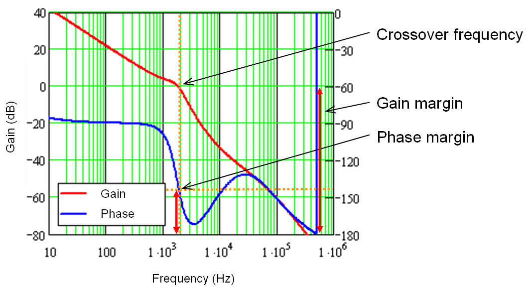
Figure 8: Bode plots for loop stability
Cross over frequency fc : The point at where the injected signal comes back at the same amplitude (0dB) is called cross over frequency or unity gain frequency.
Phase margin Øm is defined as the difference (in degrees) between the total phase shift of the feedback signal and the -180° measured at the cross over frequency
The gain margin Gc is the amount of negative gain (attenuation) where the total phase shift is 180 degree.
Sufficient phase margin is required to prevent oscillations. The step response, Figure 9, can be seen in a second order system where the damping factor is ξ ≡ øm/100.
Optimal phase margin is at 52° degrees (blue graph). Lower phase margin leads to under damped system response (red graph) and higher phase margin leads to over damped system response (green graph).
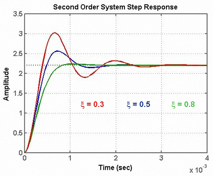
Figure 9: Second order system step response
As mentioned before, there are two main parameters that give a figure of merit of how stable the system is: Phase margin and Gain Margin. In Theory even 20° of phase margin in worst case condition could be enough for a stable design; however more degrees of margin will ensure a stable loop in any conditions. When we specify and measure the phase margin we also have to consider how much it will degrade in worst conditions, since line load and temperature changes will tend to degrade the phase margin from nominal value.
It is also important to monitor the minimum phase shift at frequency below the cross over frequency. If the phase shift gets close to 0, the system can oscillate when the gain decreases, for example with an increase of load or decrease of line voltage.
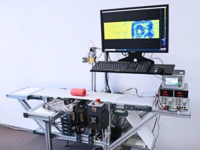
A network analyser is used for this measurement, by injecting the sinusoidal output signal into the control loop, with a sweep frequency from few tens of hertz to above the operating switching frequency and measuring two signals A and B as shown in Figure 10.

The sinusoidal signal is injected through an isolation transformer. In order to not distort the close loop system too much, the injected signal has an amplitude of few tens to hundred of mV. A resistor is connected in parallel with the output of the transformer.The two output channels of the network analyser are connected at the connection points of the transformer to measure the loop input (ch B) and loop output (ch A). Gain and phase of the function chA/chB is plotted in a logarithm scale over frequency.
The isolation transformer is needed to ensure a floating sinusoidal voltage injected to the feedback loop across an inserted resistor of few ohms. The resistor connected in parallel with the output of the transformer is in series with the feedback resistor divider and should have a resistance value much lower than the feedback resistors in order to not change the DC output voltage. The transformer should have low primary to secondary capacitance and flat frequency response. Transformers designed for this purpose are available in the market and are typically sold for few hundred Euros. However, a simple transformer can be self-made by winding two strands of wires in a toroid core.
About the author
 Michele Sclocchi is technical marketing for power management products. Sclocchi is based at Texas Instrument Sales office in Milan , Italy .
Sclocchi joined National Semiconductor in 2000. He is a specialist in switching power supply, responsible for the new products definition in the renewable energy area.
Michele Sclocchi holds a Master Degree in Electrical Engineering from the Politechnic University of Milan/Italy. He has authored over 95 publications in power electronics.
 If you enjoyed this article, you will like the following ones: don't miss them by subscribing to :