Four-switch buck-boost converter in buck or boost mode delivers the highest efficiency
Introduction
Buck-boost converters are popular solutions to cope with a wide-input voltage range that fluctuates below or above the desired output voltage. The conventional two-switch buck-boost converter offers low cost and simple control. However, it suffers from high current stress and high conduction loss, resulting in low efficiency. The excessive power dissipation associated with low efficiency makes the conventional two-switch buck-boost converter impractical for high-power applications.
A four-switch buck-boost converter benefits from synchronous rectification and thus outperforms its two-switch counterpart in terms of efficiency and power capability. Moreover, as a cascaded combination of a buck converter followed by a boost converter, a four-switch buck-boost converter can operate in buck mode or boost mode rather than conventional buck-boost mode. As such, its efficiency can be further improved.
Two-switch buck-boost converter principles of operation
Figure 1 shows a conventional two-switch buck-boost converter. The power stage consists of two switches (Q1 and Q2), two diodes (D1 and D2), a single inductor (L1), and input and output capacitors.
In buck-boost mode, MOSFETs Q1 and Q2 share a gate-control signal and turn on and off simultaneously. When Q1 and Q2 are turned on, the input voltage (VIN) is applied to the inductor (L1) and the energy is stored in the inductor. In this stage, the output capacitor supplies the entire load current. When Q1 and Q2 are turned off, diodes D1 and D2 are forward-biased; thus the inductor current ramps down at a rate proportional to VOUT. In this stage, energy is transferred from the inductor to the output load and capacitor. Figure 2 shows the current waveforms in continuous conduction mode (CCM).

Figure 1: Two-switch buck-boost converter

Figure 2: Ideal current waveforms of a two-switch buck-boost converter in CCM
The two-switch buck-boost converter uses diode rectification, also commonly known as non-synchronous rectification. With inductor current ripple neglected, the approximate conduction loss in each diode (D1 or D2) can be expressed as Equation 1:
![]()
where D is the switch (Q1/Q2) duty cycle and equals to VOUT/(VIN+VOUT), and VF is the diode (D1/D2) forward-voltage drop.
The forward-voltage drop of a typical Schottky diode is around 0.6 V, and the diode conduction loss could be significant in high-current applications. In applications where conduction loss contributes significantly or even dominates the total power loss, the efficiency suffers.
Efficiency improvement with synchronous rectification
A synchronous rectification scheme, wherein MOSFET replaces diode, is widely used in buck converters to improve efficiency. A buck-boost converter can also benefit from this scheme. By replacing diodes D1 and D2 of the two-switch buck-boost converter in Figure 1 with MOSFETs Q3 and Q4, the two-switch buck-boost converter becomes a four-switch buck-boost converter (Figure 3). The four-switch buck-boost converter features synchronous rectification. When operating in buck-boost mode, Q3 and Q4 share a gate-control signal, which is complementary to the gate-control signal of Q1 and Q2 (Figure 4).

Figure 3: Four-switch buck-boost converter

Figure 4: Gate-control signals in buck-boost mode
The principle of operation of the four-switch buck-boost converter in CCM is similar to that of the two-switch buck-boost converter shown in Figure 2. The current flow through the synchronous MOSFETs (Q3 and Q4) resembles that of D1 and D2. Equation 2 estimates the conduction loss of each synchronous MOSFET (Q3 or Q4):
![]()
where RDSON is the on-resistance of the synchronous MOSFET. Equation 3 gives the voltage drop across the on-resistance:
![]()
Equation 2 can then be rearranged as Equation 4:
![]()
Comparing Equation 4 to Equation 1 reveals that the conduction loss difference between non-synchronous rectification (diode) and synchronous rectification (MOSFET) is determined by the voltage difference between VF and VSR. VSR is often much smaller than VF, since the MOSFET on-resistance is very low. For instance, the on-resistance of a 25-V MOSFET is as low as 1.5 mOhm, which only generates a 15-mV drop with 10-A current flowing through. 15 mV of VSR certainly introduces much lower conduction loss than 0.6 V of VF, and therefore the efficiency can be improved.
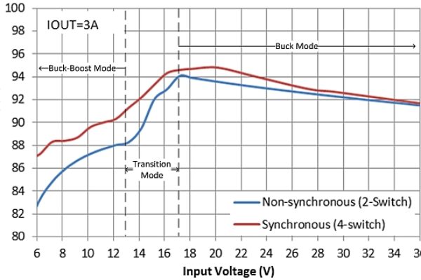
Figure 5 shows the efficiency comparison between four-switch (synchronous) and two-switch (non-synchronous) buck-boost converters. The nominal output voltages are both 12V. I measured the efficiency data of two designs using the LM5118 buck-boost controller from Texas Instruments (TI). Since the LM5118 is a two-switch buck-boost controller, I used two additional driver ICs along with the controller to drive four MOSFETs in a synchronous configuration.

Figure 5: Efficiency comparison between four-switch and two-switch buck-boost converters
The four-switch buck-boost converter gains more efficiency than the two-switch buck-boost converter by reducing conduction loss. The lower the VIN, the more the conduction loss contributes to total loss. As a result, efficiency improves more at low VIN than at higher VIN.
However, the efficiency at low VIN is generally lower than that at high VIN, regardless of whether the converter is two-switch or four-switch. This is because the LM5118 controller has different operation modes. The converter operates in buck mode when VIN is above 17 V, while it operates in buck-boost mode when VIN falls below 13.2 V. The efficiency in buck mode is higher than that in buck-boost mode. Actually, the efficiency at low VIN can be further improved by optimizing the operation mode. I will elaborate on the impact of operation mode on efficiency in the following section.
Operation-mode optimization of a four-switch buck-boost converter
With the control scheme in Figure 4, the four-switch buck-boost converter (Figure 3) operates in buck-boost mode. In this operation mode, all four switches (Q1, Q2, Q3 and Q4) are switching and generating switching loss in each switching period. Moreover, all four switches – as well as inductor L1 – see a current stress of IIN+IOUT with inductor ripple current neglected, which results in a large conduction loss. Such large switching and conduction losses in buck-boost mode make the buck-boost converter not as efficient as a buck or boost converter.
Fortunately, the four-switch buck-boost converter is a cascaded combination of a buck converter followed by a boost converter. When implementing the optimized control scheme in Figure 6, the four-switch buck-boost converter in Figure 3 works as the equivalent circuits in Figure 7. When VIN is higher than VOUT, Q2 is kept off while Q4 is always off; thus, it works like a typical buck converter. In contrast, when VIN is lower than VOUT, Q1 is always on while Q3 is kept off; it then works as a typical boost converter. Figure 8 shows the corresponding operation waveforms.

Figure 6: Gate-control signals in buck mode or boost mode

Figure 7: Equivalent circuits in buck or boost mode

Figure 8: Current waveforms of a four-switch buck-boost converter in CCM
Table 1 compares the three different operation modes. In buck-boost mode, two more switches are switching in each period, compared to buck mode and boost mode. More switches switching in each period essentially generates more switching loss. Furthermore, the average or pedestal current flowing through inductors and switches in buck-boost mode (IIN+IOUT) is higher than that in both buck mode (IOUT) and boost mode (IIN), which results in higher conduction loss. As a result, the efficiency in buck-boost mode is lowest.

Table 1: Operation mode comparison
Improved four-switch buck-boost efficiency by optimized operation mode
You can successfully implement a four-switch buck-boost converter using a buck- or boost-mode control scheme with the LM5175 controller from TI. The schematic and photo of the evaluation module (EVM) are shown in Figure 9 and Figure 10, respectively. The input voltage ranges from 6 V to 36 V, while the output voltage is 12 V with 10 A of nominal output current. Figure 11 shows the efficiency and power loss at full load with respect to input voltage. Very high (94 percent and above) efficiency has been achieved over the entire input-voltage range, and the peak efficiency is up to 98.3 percent.

Figure 9: Four-switch buck-boost converter schematic

Figure 10: Four-switch buck-boost converter evaluation module

Figure 11: Efficiency and power loss versus input voltage
Conclusions
A buck-boost converter is required to maintain output-voltage regulation in applications where the input voltage could be either higher or lower than the desired output voltage. The conventional two-switch buck-boost converter suffers from low efficiency and has limited output-power capability. Synchronous rectification, along with an optimized buck or boost operation mode, reduces the conduction and switching losses in a four-switch buck-boost converter, enabling you to achieve the highest efficiency.
References
LM5175 wide VIN four-switch buck-boost converter high power evaluation module user’s guide, Texas Instruments, February 2015.
AN-2178 LM5118 Four Switch Conversion, Application Report, Texas Instruments, May 2013.
Download these datasheets: LM5175, LM5118.
 If you enjoyed this article, you will like the following ones: don't miss them by subscribing to :